MicroMod Teensy Processor Hookup Guide a learn.sparkfun.com tutorial
Available online at: http://sfe.io/t1266
Introduction
The SparkFun MicroMod Teensy Processor leverages the awesome computing power of the NXP iMXRT1062 chip and pairs it with the M.2 MicroMod connector to allow you to plug it into your choice of compatible MicroMod Carrier Board.

On top of excellent processing power and speed, the Teensy Processor offers a plethora of interface options including multiple serial UARTs as well as two I2C and SPI buses. Along with these standard interfaces, the Teensy Processor Board also features USB Host capability, a CAN-Bus and a digital audio interface.
Required Materials
Along with your MicroMod Teensy Processor, you'll need a Carrier Board to plug your Processor into. SparkFun offers a variety of MicroMod Carrier Boards to fit your project's needs:


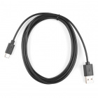
You'll also need a USB-C cable to connect the Carrier to your computer and if you want to add some Qwiic breakouts to your MicroMod project you'll want at least one Qwiic cable. Below are some options for both of those cables:

Depending on which Carrier Board you choose, you may need a few extra peripherals to take full advantage of them. Refer to the Carrier Boards' respective Hookup Guides for specific recommendations.
Suggested Reading
The SparkFun MicroMod ecosystem offers a unique way to allow users to customize their project to their needs. Do you want to send your weather data via a wireless signal (e.g. Bluetooth or WiFi)? There's a MicroMod Processor for that. Looking to instead maximize efficiency and processing power? You guessed it, there's a MicroMod Processor for that. If you are not familiar with the MicroMod ecosystem, take a look here:
If you aren't familiar with the MicroMod ecosystem, we recommend reading here for an overview:
| MicroMod Ecosystem |
We also recommend reading through the following tutorials if you are not familiar with the concepts covered in them:
Serial Communication
Serial Peripheral Interface (SPI)
Installing Arduino IDE
Getting Started with the Teensy
Getting Started with MicroMod
Hardware Overview
We'll cover the hardware and components included on the MicroMod Teensy Processor Board in this section and highlight some of their unique features.
M.2 Connector
All of our MicroMod Processor come equipped with the M.2 MicroMod Connector, which leverages the M.2 standard and specification to allow you to install your MicroMod Processor on your choice of Carrier Board.
 |  |
| M.2 Connector from the Front | M.2 Connector from the Back |
The M.2 MicroMod connector is keyed (in tandem the set screw notch) to prevent the Processor from being inserted and secured improperly.
NXP iMXRT1062 Processor
The brain of the MicroMod Teensy Processor is the NXP iMXRT1062 from NXP Semiconductors. This Arm Cortex-M7 core processor is one of the most powerful microprocessors available today. The Teensy Processor takes advantage of the following properties:
- ARM Cortex-M7 at 600MHz
- Up to 600MHz clock frequency
- 3 Serial Ports (1 dedicated USB, 2 Serial UART)
- 2 SPI ports (One dedicated SPI available by default on most Carrier Boards[1]. Dedicated Hardware SDIO for SD.)
- 2 I2C Ports (One I2C bus available by default on most Carrier Boards[1])
- USB Host Capability
- 1 CAN Bus Interface
- 1 I2S Digital Audio
- 12 Dedicated GPIO
- 14 Analog pins (2 dedicated, 10 share signals.)
- 3.3V-tolerant I/O pins
- 8MB Flash Memory (64l reserved for recover & EEPROM emulation)
- 1024K RAM Memory (512K is tightly coupled)

Flash IC
The MicroMod Teensy Processor uses the W25Q128JV-DTR serial flash memory IC from Windbond Electronics. The flash IC features 128mb of memory. For a detailed overview of the IC, refer to the datasheet.

LEDs
There are two LEDs on the Teensy Processor. The PROG LED indicates when the HalfKay bootloader is enabled and the programming IC is powered. We'll cover how to enter the bootloader in the Software Setup and Arduino Example sections. The STAT LED is tied to SCK/13 and can be used as a status LED or as a built-in LED. Control it directly by writing to LED_BUILTIN.

Measure Jumper
The Measure (MEAS) Jumper can be opened to measure how much current the Teensy Processor is pulling from V_USB. It's is CLOSED by default and ties the USB_VBUS pins to V_USB. Open it by severing the trace and then use a digital multimeter to measure the current draw.

Teensy Processor Pin Functions
The Teensy Processor is similar to the Teensy 4.0 and 4.1 with a few notable differences. In order to maintain easy interoperability with MicroMod Carrier Boards, not all of the alternate pin functions are defined for the MicroMod Teensy board variant but we have done our best to make the Teensy Processor as versatile as possible with the right Carrier Board. The sections below outline the various signal protocols available on the MicroMod Teensy.
I2C
As you may have guessed from our extensive Qwiic System, we love communicating with devices using I2C! The Teensy Processor features two I2C buses. The main I2C bus has dedicated pins connected to MiroMod pads 12 (SDA) and 14 (SCL) (Teensy pins 18 and 19), along with a dedicated interrupt pin connected to MicroMod pad 16 (Teensy pin 29). The primary I2C Bus will almost always be connected to a Qwiic connector on your Carrier Board.
If you need a second I2C bus, the Teensy has SDA1 and SCL1 on MicroMod pads 51 and 51 (Teensy pins 25 and 24). To use this second bus, initialize it by calling Wire1.begin();.
UART
The Teensy Processor has three UARTs available. The primary UART is tied to USB_D&plusmin; (MicroMod pads 3 and 5) for serial communication over USB. This is used for your standard serial upload as well as serial prints in Arduino. The secondary UART is a hardware UART tied to MicroMod pads 19 (RX1) and 17 (TX1) (Teensy pins 0 and 1). The tertiary UART is another hardware UART tied to MicroMod pads 20 (RX2) and 22 (TX2) (Teensy pins 17 and 16). In Arduino, the three UARTs are called as listed below:
Serial- Communication over USBSerial1- Communication over RX1/TX1Serial2- Communication over RX2/TX2
SPI
The Teensy Processor has two SPI buses. The primary SPI bus connects to the following pins:
- SDI/CIPO - Serial data input (Controller In/Peripheral Out). MicroMod pad 61. Teensy pin 12.
- SDO/COPI - Serial data output (Controller Out/Peripheral In). MicroMod pad 59. Teensy pin 11.
- SCK - SPI Clock. MicroMod pad 57. Teensy pin 13.
- CS - Chip select. MicroMod pad 55. Teensy pin 10.
Due to hardware limitations on most MicroMod Carrier Boards, SPI1 is only available for hardware SDIO communication with an SD card. Use the ATP Carrier to directly interact with SPI1.
CAN-Bus
One of the unique features of the Teensy is its ability to communicate with CAN devices. The Teensy MicroMod can receive CAN messages but in order to send them properly you will need a separate CAN transceiver. CAN-RX is tied to MicroMod pad 41 (Teensy pin 30) and CAN-TX is tied to MicroMod pad 43 (Teensy pin 31).
AUDIO
The Teensy Processor supports audio using the I2S standard. The pins used are:
- AUD_OUT - GPIO pin 17, pad 56 on the MicroMod, this is the digital audio output.
- AUD_IN - GPIO pin 16, pad 54 on the MicroMod, this is the digital audio input.
- AUD_LRCLK - GPIO pin 25, pad 52 on the MicroMod. Officially called "word select", and also known as "frame sync".
- AUD_BCLK - GPIO pin 26, pad 50 on the MicroMod. Offically called "continuous serial clock, and also known as the "bit clock"
GPIO/BUS
The MicroMod Teensy has all 12 general purpose IO pins available on top of 6 dedicated pins for digital, analog and PWM signals. The dedicated pins are just that, and are not shared with any other pin, unlike the general purpose pins which may be shared with other pins. Take note that not all GPIO pins are broken out or in use on every carrier board. Refer to your Carrier Board's Hookup Guide for more information on pin use.
Dedicated Pins
- A0 - Teensy pin 14, MicroMod pad 34
- A1 - Teensy pin 15, MicroMod pad pad 38
- D0 - Teensy pin 4, MicroMod pad pad 10
- D1 - Teensy pin 5, MicroMod pad pad 18
- PWM0 - Teensy pin 3, MicroMod pad pad 32
- PWM1 - Teensy pin 2, MicroMod pad pad 47
General Purpose IO pins
- G0 - GPIO pin 15, pad 40 on the MicroMod
- G1 - GPIO pin 25, pad 42 on the MicroMod
- G2 - GPIO pin 26, pad 44 on the MicroMod
- G3 - GPIO pin 17, pad 46 on the MicroMod
- G4 - GPIO pin 16, pad 48 on the MicroMod
- G5 - GPIO pin 32, pad 73 on the MicroMod
- G6 - GPIO pin 33, pad 71 on the MicroMod
Extra Teensy Functionality
As experienced users may know, the pins on Teensy development boards are very versatile and can be used for a multitude of purposes. As we noted above, in order to maintain compatibility with the rest of the MicroMod system, not all of these alternate functions are available on the MicroMod Teensy but some pins can be configured for things like Analog Inputs or Pulse Width Modulation. As mentioned before, the best way to interact with these pins is with the ATP Carrier Board.
The list below shows all 14 pins on the Teensy Processor available for use as Analog Inputs.
- A0 - Teensy pin 14, dedicated on MM pad 34. PWM-Capable.
- A1 - Teensy pin 15, dedicated on MM pad 38. PWM-Capable.
- A2 - Teensy pin 16, shared with RX2 (MMpad 20). Input Only.
- A3 - Teensy pin 17, shared with TX2 (MM pad 22). Input Only.
- A4 - Teensy pin 18, shared with I2C_SDA (MM pad 12). PWM-Capable.
- A5 - Teensy pin 19, shared with I2C_SCL (MM pad 14). PWM-Capable.
- A6 - Teensy pin 20, shared with AUD_LRCLK (MM pad 52). Input Only.
- A7 - Teensy pin 21, shared with AUD_BCLK (MM pad 50). Input Only.
- A8 - Teensy pin 22, shared with BATT_VIN/3 (MM pad 49). Input Only.
- A9 - Teensy pin 23, shared with AUD_MCLK (MM pad 58). PWM-Capable.
- A10 - Teensy pin 24, shared with I2C_SCL1 (MM pad 53). PWM-Capable.
- A11 - Teensy pin 25, shared with I2C_SDA1 (MM pad 51). PWM-Capable.
- A12 - Teensy pin 26, shared with G8 (MM pad 67). Input Only.
- A13 - Teensy pin 27, shared with G11 (MM pad 8). Input Only.
The default MicroMod Teensy Processor board definition is limited to these extra functionalities along with a few other pins that can technically be used for PWM signals when not in use for other signal protocols. Keep reading to the next section, MicroMod Pinout, for specific information on these pins.
MicroMod Pinout
Refer to the datasheet and user manual for a full overview of the iMXRT1062's capabilities. The complete pin map can be found in the table below or you can refer to the schematic.
| AUDIO | UART | GPIO/BUS | I2C | SDIO | SPI | Dedicated |
| Teensy Pin | Alternate Function | Primary Function | Bottom Pin | Top Pin | Primary Function | Alternate Function | Teensy Pin |
|---|---|---|---|---|---|---|---|
| (Not Connected) | 75 | GND | |||||
| 3.3V | 74 | 73 | G5 | 45 | |||
| RTC_3V_BATT | 72 | 71 | G6 | PWM | 6 | ||
| 39 | SDIO_DATA3 | 70 | 69 | G7 | PWM | 9 | |
| 38 | SDIO_DATA2 | 68 | 67 | G8 | A12 (Input only) | 26 | |
| 34 | SDIO_DATA1 | 66 | 65 | G9 | 32 | ||
| 35 | SDIO_DATA0 | 64 | 63 | G10 | PWM | 33 | |
| 37 | SDIO_CMD | 62 | 61 | SPI_CIPO | PWM | 12 | |
| 36 | SDIO_SCK | 60 | 59 | SPI_COPI | PWM | 11 | |
| 23 | A9 (PWM) | AUD_MCLK | 58 | 57 | SPI_SCK | STAT LED / PWM | 13 |
| 7 | PWM | AUD_OUT | 56 | 55 | SPI_CS | PWM | 10 |
| 8 | PWM | AUD_IN | 54 | 53 | I2C_SCL1 | A10 (PWM) | 24 |
| 20 | A6 (Input Only) | AUD_LRCLK | 52 | 51 | I2C_SDA1 | A11 (PWM) | 25 |
| 21 | A7 (Input Only)> | AUD_BCLK | 50 | 49 | BATT_VIN / 3 (0 to 3.3V) | A8 (Input Only) | 22 |
| 44 | G4 | 48 | 47 | PWM1 | 2 | ||
| 43 | G3 | 46 | 45 | GND | |||
| 42 | G2 | 44 | 43 | CAN_TX | 31 | ||
| 42 | G1 | 42 | 41 | CAN_RX | 30 | ||
| 40 | G0 | 40 | 39 | GND | |||
| 15 | PWM | A1 | 38 | 37 | USBHOST_D+ | USB2_D+ | |
| GND | 36 | 35 | USBHOST_D- | USB2_D- | |||
| 14 | PWM | A0 | 34 | 33 | GND | ||
| 3 | PWM0 | 32 | 31 | Module Key | |||
| Module Key | 30 | 29 | Module Key | ||||
| Module Key | 28 | 27 | Module Key | ||||
| Module Key | 26 | 25 | Module Key | ||||
| Module Key | 24 | 23 | Not Connected | ||||
| 17 | A3 (Input Only) | UART_TX2 | 22 | 21 | Not Connected | ||
| 17 | A3 (Input Only) | UART_RX2 | 20 | 19 | UART_RX1 | 0 | |
| 5 | PWM | D1 | 18 | 17 | UART_TX1 | PWM | 1 |
| 29 | PWM | I2C_INT | 16 | 15 | Not Connected | ||
| 19 | A5 (PWM) | I2C_SCL | 14 | 13 | Not Connected | ||
| 18 | A4 (PWM) | I2C_SDA | 12 | 11 | BOOT (Open Drain) | PROG | |
| 4 | PWM | D0 | 10 | 9 | USB_VIN | V_USB | |
| 27 | A13 (Input Only) | G11 | 8 | 7 | GND | ||
| ON/OFF | RESET# (Open Drain) | 6 | 5 | USB_D+ | USB_D+ | ||
| 28 | 3.3V_EN | 4 | 3 | USB_D- | USB_D- | ||
| 3.3V | 2 | 1 | GND |
| Function | Bottom Pin | Top Pin | Function | ||||||
|---|---|---|---|---|---|---|---|---|---|
| (Not Connected) | 75 | GND | |||||||
| 3.3V | 74 | 73 | G5 / BUS5 | ||||||
| RTC_3V_BATT | 72 | 71 | G6 / BUS6 | ||||||
| SPI_CS1# | SDIO_DATA3 (I/O) | 70 | 69 | G7 / BUS7 | |||||
| SDIO_DATA2 (I/O) | 68 | 67 | G8 | ||||||
| SDIO_DATA1 (I/O) | 66 | 65 | G9 | ADC_D- | CAM_HSYNC | ||||
| SPI_CIPO1 | SDIO_DATA0 (I/O) | 64 | 63 | G10 | ADC_D+ | CAM_VSYNC | |||
| SPI COPI1 | SDIO_CMD (I/O) | 62 | 61 | SPI_CIPO (I) | |||||
| SPI SCK1 | SDIO_SCK (O) | 60 | 59 | SPI_COPI (O) | LED_DAT | ||||
| AUD_MCLK (O) | 58 | 57 | SPI_SCK (O) | LED_CLK | |||||
| CAM_MCLK | PCM_OUT | I2S_OUT | AUD_OUT | 56 | 55 | SPI_CS# | |||
| CAM_PCLK | PCM_IN | I2S_IN | AUD_IN | 54 | 53 | I2C_SCL1 (I/O) | |||
| PDM_DATA | PCM_SYNC | I2S_WS | AUD_LRCLK | 52 | 51 | I2C_SDA1 (I/O) | |||
| PDM_CLK | PCM_CLK | I2S_SCK | AUD_BCLK | 50 | 49 | BATT_VIN / 3 (I - ADC) (0 to 3.3V) | |||
| G4 / BUS4 | 48 | 47 | PWM1 | ||||||
| G3 / BUS3 | 46 | 45 | GND | ||||||
| G2 / BUS2 | 44 | 43 | CAN_TX | ||||||
| G1 / BUS1 | 42 | 41 | CAN_RX | ||||||
| G0 / BUS0 | 40 | 39 | GND | ||||||
| A1 | 38 | 37 | USBHOST_D- | ||||||
| GND | 36 | 35 | USBHOST_D+ | ||||||
| A0 | 34 | 33 | GND | ||||||
| PWM0 | 32 | 31 | Module Key | ||||||
| Module Key | 30 | 29 | Module Key | ||||||
| Module Key | 28 | 27 | Module Key | ||||||
| Module Key | 26 | 25 | Module Key | ||||||
| Module Key | 24 | 23 | SWDIO | ||||||
| UART_TX2 (O) | 22 | 21 | SWDCK | ||||||
| UART_RX2 (I) | 20 | 19 | UART_RX1 (I) | ||||||
| CAM_TRIG | D1 | 18 | 17 | UART_TX1 (0) | |||||
| I2C_INT# | 16 | 15 | UART_CTS1 (I) | ||||||
| I2C_SCL (I/0) | 14 | 13 | UART_RTS1 (O) | ||||||
| I2C_SDA (I/0) | 12 | 11 | BOOT (I - Open Drain) | ||||||
| D0 | 10 | 9 | USB_VIN | ||||||
| SWO | G11 | 8 | 7 | GND | |||||
| RESET# (I - Open Drain) | 6 | 5 | USB_D- | ||||||
| 3.3V_EN | 4 | 3 | USB_D+ | ||||||
| 3.3V | 2 | 1 | GND | ||||||
| Signal Group | Signal | I/O | Description | Voltage | Power | 3.3V | I | 3.3V Source | 3.3V |
|---|---|---|---|---|
| GND | Return current path | 0V | ||
| USB_VIN | I | USB VIN compliant to USB 2.0 specification. Connect to pins on processor board that require 5V for USB functionality | 4.8-5.2V | |
| RTC_3V_BATT | I | 3V provided by external coin cell or mini battery. Max draw=100μA. Connect to pins maintaining an RTC during power loss. Can be left NC. | 3V | |
| 3.3V_EN | O | Controls the carrier board's main voltage regulator. Voltage above 1V will enable 3.3V power path. | 3.3V | |
| BATT_VIN/3 | I | Carrier board raw voltage over 3. 1/3 resistor divider is implemented on carrier board. Amplify the analog signal as needed for full 0-3.3V range | 3.3V | |
| Reset | Reset | I | Input to processor. Open drain with pullup on processor board. Pulling low resets processor. | 3.3V |
| Boot | I | Input to processor. Open drain with pullup on processor board. Pulling low puts processor into special boot mode. Can be left NC. | 3.3V | |
| USB | USB_D± | I/O | USB Data ±. Differential serial data interface compliant to USB 2.0 specification. If UART is required for programming, USB± must be routed to a USB-to-serial conversion IC on the processor board. | |
| USB Host | USBHOST_D± | I/O | For processors that support USB Host Mode. USB Data±. Differential serial data interface compliant to USB 2.0 specification. Can be left NC. | |
| CAN | CAN_RX | I | CAN Bus receive data. | 3.3V |
| CAN_TX | O | CAN Bus transmit data. | 3.3V | |
| UART | UART_RX1 | I | UART receive data. | 3.3V |
| UART_TX1 | O | UART transmit data. | 3.3V | |
| UART_RTS1 | O | UART request to send. | 3.3V | |
| UART_CTS1 | I | UART clear to send. | 3.3V | |
| UART_RX2 | I | 2nd UART receive data. | 3.3V | |
| UART_TX2 | O | 2nd UART transmit data. | 3.3V | |
| I2C | I2C_SCL | I/O | I2C clock. Open drain with pullup on carrier board. | 3.3V |
| I2C_SDA | I/O | I2C data. Open drain with pullup on carrier board | 3.3V | |
| I2C_INT# | I | Interrupt notification from carrier board to processor. Open drain with pullup on carrier board. Active LOW | 3.3V | |
| I2C_SCL1 | I/O | 2nd I2C clock. Open drain with pullup on carrier board. | 3.3V | |
| I2C_SDA1 | I/O | 2nd I2C data. Open drain with pullup on carrier board. | 3.3V | |
| SPI | SPI_COPI | O | SPI Controller Output/Peripheral Input. | 3.3V |
| SPI_CIPO | I | SPI Controller Input/Peripheral Output. | 3.3V | |
| SPI_SCK | O | SPI Clock. | 3.3V | |
| SPI_CS# | O | SPI Chip Select. Active LOW. Can be routed to GPIO if hardware CS is unused. | 3.3V | |
| SPI/SDIO | SPI_SCK1/SDIO_CLK | O | 2nd SPI Clock. Secondary use is SDIO Clock. | 3.3V |
| SPI_COPI1/SDIO_CMD | I/O | 2nd SPI Controller Output/Peripheral Input. Secondary use is SDIO command interface. | 3.3V | |
| SPI_CIPO1/SDIO_DATA0 | I/O | 2nd SPI Peripheral Input/Controller Output. Secondary use is SDIO data exchange bit 0. | 3.3V | |
| SDIO_DATA1 | I/O | SDIO data exchange bit 1. | 3.3V | |
| SDIO_DATA2 | I/O | SDIO data exchange bit 2. | 3.3V | |
| SPI_CS1/SDIO_DATA3 | I/O | 2nd SPI Chip Select. Secondary use is SDIO data exchange bit 3. | 3.3V | |
| Audio | AUD_MCLK | O | Audio master clock. | 3.3V |
| AUD_OUT/PCM_OUT/I2S_OUT/CAM_MCLK | O | Audio data output. PCM synchronous data output. I2S serial data out. Camera master clock. | 3.3V | |
| AUD_IN/PCM_IN/I2S_IN/CAM_PCLK | I | Audio data input. PCM syncrhonous data input. I2S serial data in. Camera periphperal clock. | 3.3V | |
| AUD_LRCLK/PCM_SYNC/I2S_WS/PDM_DATA | I/O | Audio left/right clock. PCM syncrhonous data SYNC. I2S word select. PDM data. | 3.3V | |
| AUD_BCLK/PCM_CLK/I2S_CLK/PDM_CLK | O | Audio bit clock. PCM clock. I2S continuous serial clock. PDM clock. | 3.3V | |
| SWD | SWDIO | I/O | Serial Wire Debug I/O. Connect if processor board supports SWD. Can be left NC. | 3.3V |
| SWDCK | I | Serial Wire Debug clock. Connect if processor board supports SWD. Can be left NC. | 3.3V | |
| ADC | A0 | I | Analog to digital converter 0. Amplify the analog signal as needed to enable full 0-3.3V range. | 3.3V |
| A1 | I | Analog to digital converter 1. Amplify the analog signal as needed to enable full 0-3.3V range. | 3.3V | |
| PWM | PWM0 | O | Pulse width modulated output 0. | 3.3V |
| PWM1 | O | Pulse width modulated output 1. | 3.3V | |
| Digital | D0 | I/O | General digital input/output pin. | 3.3V |
| D1/CAM_TRIG | I/O | General digital input/output pin. Camera trigger. | 3.3V | |
| General/Bus | G0/BUS0 | I/O | General purpose pins. Any unused processor pins should be assigned to Gx with ADC + PWM capable pins given priority (0, 1, 2, etc.) positions. The intent is to guarantee PWM, ADC and Digital Pin functionality on respective ADC/PWM/Digital pins. Gx pins do not guarantee ADC/PWM function. Alternative use is pins can support a fast read/write 8-bit or 4-bit wide bus. | 3.3V |
| G1/BUS1 | I/O | 3.3V | ||
| G2/BUS2 | I/O | 3.3V | ||
| G3/BUS3 | I/O | 3.3V | ||
| G4/BUS4 | I/O | 3.3V | ||
| G5/BUS5 | I/O | 3.3V | ||
| G6/BUS6 | I/O | 3.3V | ||
| G7/BUS7 | I/O | 3.3V | ||
| G8 | I/O | General purpose pin | 3.3V | |
| G9/ADC_D-/CAM_HSYNC | I/O | Differential ADC input if available. Camera horizontal sync. | 3.3V | |
| G10/ADC_D+/CAM_VSYNC | I/O | Differential ADC input if available. Camera vertical sync. | 3.3V | |
| G11/SWO | I/O | General purpose pin. Serial Wire Output | 3.3V |
Board Dimensions
MicroMod Processors all measure in at 22mm x 22mm, with 15mm to the top notch and 12mm to the E key. For more information regarding the processor board physical standards, head on over to the Getting Started with MicroMod and Designing With MicroMod tutorials.

Hardware Assembly
Now that we are familiar with the components on the Teensy Processor, it's time to assemble it with your chosen MicroMod Carrier Board and connect it to your computer.
Inserting the Processor Board
With the M.2 MicroMod connector, connecting your Processor is a breeze. Simply match up the key on your Processor's beveled edge connector to the key on the M.2 connector. At a 45° angle, insert the processor board to the M.2 connector. The Processor Board will stick up at an angle as shown here:

Once the board is in the socket, gently press the Processor down, grab the set screw and tighten it with a Phillip's head screwdriver:

Once the Processor is secure, your assembled MicroMod system should look similar to the image below.

Connecting Everything Up
Depending on which Carrier Board you are using with your Teensy Processor, plug in any other devices (Qwiic breakouts, UART devices, SD cards, I/O devices, etc.) prior to plugging in your Carrier Board to USB. Refer to your Carrier Board's Hookup Guide for specific instructions for Hardware Assembly.
With your Teensy Processor Board inserted and secured and your other devices connected properly it's time to connect your MicroMod Carrier Board to your computer using the USB-C connector. On first power-up, the STAT LED on your Teensy Processor should be blinking on and off every second.
Software Setup
To start working with the Teensy Processor (or any Teensy really), all you need to do is plug in your USB cable to your computer and your Carrier Board. There are two options for programming the Teensy boards - the Arduino IDE or your favorite C compiler. This tutorial will demonstrate how to use Arduino with the Teensy Processor so if you prefer to not use Arduino, download and install the Teensy Loader application.
Arduino IDE Installation
If this is your first time using Arduino, please review our tutorial on installing the Arduino IDE. If you have not previously installed an Arduino library, please check out our installation guide. With Arduino installed, move on to installing the Teensyduino add-on.
Teensyduino Installation
With Arduino installed, download and install the Teensyduino add-on before uploading code to the Teensy Processor. You can find the Teensyduino download for Windows, Mac OS X and Linux from PJRC here.
Teensyduino includes all Teensy board definitions as well as an optional installation of a selection of Arduino libraries to work with Teensy boards. Please follow their installation instructions for the most up-to-date version of the Teensyduino for your operating system. During installation, select which Teensy-compatible libraries you'd like to install. If you aren't sure which libraries you will want, you can skip this step and download and install them later from their curated list.
Programming the Teensy
Open up the Arduino IDE, select the Teensy MicroMod board from the Board menu and select the Port your Processor Board enumerated on. With everything selected properly, press the BOOT button on your Carrier Board to manually enter the bootloader. You should see this window:

Once the Teensy is in the bootloader, upload the code to your board as usual through Arduino. Press the BOOT button on the Carrier Board once Arduino has compiled the code to complete the upload if prompted. You should only need to do this the first time you upload code on every power cycle.
Arduino Example: Blink
With the MicroMod Teensy Processor Board Definitions installed, let's do a quick code upload to make sure everything went correctly during the Arduino Software Setup.
Selecting and Loading Blink
We'll start off with a basic Blink example to turn the STAT LED on and off just to make sure everything is working properly and your Processor can accept code.
Open up the Arduino IDE and select the "Blink" example by navigating to "File > Examples > 01.Basics > Blink" or copy the code below into a blank sketch:
language:c
// the setup function runs once when you press reset or power the board
void setup() {
  // initialize digital pin LED_BUILTIN as an output.
  pinMode(LED_BUILTIN, OUTPUT);
}

// the loop function runs over and over again forever
void loop() {
  digitalWrite(LED_BUILTIN, HIGH);   // turn the LED on (HIGH is the voltage level)
  delay(1000);                       // wait for a second
  digitalWrite(LED_BUILTIN, LOW);    // turn the LED off by making the voltage LOW
  delay(1000);                       // wait for a second
}
With the example opened, select your Board (SparkFun MicroMod Teensy Processor Board) and Port using the Tools > Board and Tools > Port menus and click the "Upload" button. Barring any issues during compilation and upload, the STAT LED on your Teensy Processor should blink on and off every second.
Note, if this is the first time uploading click the Verify button, the Teensy Loader Program will open (if it is not already open) and prompt you to push the Pushbutton (the BOOT button on your Carrier Board). After that, you can upload to the Teensy Processor just like any other Arudino by clicking the Upload button.
Troubleshooting
If your product is not working as you expected or you need technical assistance or information, head on over to the SparkFun Technical Assistance page for some initial troubleshooting.
If you don't find what you need there, the SparkFun Forums are a great place to find and ask for help. If this is your first visit, you'll need to create a Forum Account to search product forums and post questions.
Resources and Going Further
Now that you've gotten your MicroMod Teensy Processor up and running with your chosen Carrier Board, it's time to start your MicroMod project! Take a look at the following resources for more information about MicroMod and Teensy.
The links below offer more information about the Teensy Processor:
For more information on the MicroMod ecosystem, check out these resources:
For more information about Teensy, take a look at the following pages:
learn.sparkfun.com | CC BY-SA 3.0 | SparkFun Electronics | Niwot, Colorado