Multiplexer Breakout Hookup Guide a learn.sparkfun.com tutorial
Available online at: http://sfe.io/t553
Introduction
The SparkFun Multiplexer Breakout provides access to all pins and features of the 74HC4051, an 8-channel analog multiplexer/demultiplexer. The 74HC4051 allows you to turn four I/O pins into eight multi-functional, individually-selectable signals, which can be used do everything from driving eight LEDs to monitoring eight potentiometers.

A multiplexer, commonly abbreviated down to “mux”, is an electronically-actuated switch, which can turn one signal into many. It routes a common input signal to any number of separate outputs. Similarly, a demultiplexer routes any number of selectable inputs to a single common output.
The 74HC4051 can function as either a multiplexer or a demultiplexer, and it features eight channels of selectable inputs/outputs. The routing of common signal to independent I/O is set by digitally controlling three select lines, which can be set either high or low into one of eight binary combinations.
Covered In This Tutorial
This tutorial covers everything you should need to assemble the Multiplexer Breakout then wire it and integrate it into your project. Included in the tutorial are a pair of Arduino examples, which demonstrate how to use the mux for both digital output and analog input. The tutorial is split into the following sections, which you can navigate through using the bar on the right.
- 74HC4051 Breakout Overview– A quick introduction to the workings of the 74HC4051 and the extra features of the breakout board.
- Board Assembly– Tips and tricks for soldering headers or wires to your breakout and mounting it into your project.
- Arduino Example: Output– An Arduino circuit and example code demonstrating how to use the multiplexer to drive eight LEDs.
- Arduino Example: Input– Circuit and an Arduino sketch explaining how to use the board to read eight analog voltage-producing photocells.
Suggested Reading
Muxes are a great tool for electronics users of all experience levels – anyone who needs to multiply their project’s pin count. There are a few subjects you should be familiar with before diving into multiplexing, though. If the subjects below sound foreign to you, consider browsing through that tutorial before continuing on.
Binary
How to Use a Breadboard
Analog vs. Digital
74HC4051 Breakout Overview
The Multiplexer Breakout’s schematic is just about as simple as it gets: There’s the chip, a decoupling capacitor, a pull-up resistor, and all of the pins are broken out (some broken out twice):
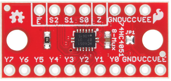
One half of the board breaks out the control signals (E, S0-S2) and common input/output (Z). The other side provides access to all eight independent I/O’s (Y0-Y7). Both sides include supply and ground connections (VCC, VEE, GND). The table below summarizes each pin and its function.
| Pin Label | Function | Input/Output (to board) | Notes |
|---|---|---|---|
| E | Enable | Input | Active low enable |
| S2, S1, S0 | Select Controls | Input | Select inputs, S2 is the msb and S0 is the lsb |
| Z | Common I/O | Input/Output | Common output or input |
| GND | Ground | Supply | Ground supply voltage (0V) |
| VCC | Positive supply | Supply | Positive supply voltage (2-10V) |
| VEE | Negative supply | Supply | Negative supply voltage (Jumpered to ground by default) |
| Y7, Y6, Y5, Y4, Y3, Y2, Y1, Y0 | Independent I/O | Input/Output | Selectable I/O to be routed to common pin |
74HC4051 Logic Table
The select pins (S2-S0), in addition to the enable pin (E), control which (if any) of the eight independent I/O pins (Y0-Y7) are connected to the common pin (Z). The function table below shows how those pins work together to select the I/O.
| E | S2 | S1 | S0 | I/O Connected to Z |
|---|---|---|---|---|
| L | L | L | L | Y0 |
| L | L | L | H | Y1 |
| L | L | H | L | Y2 |
| L | L | H | H | Y3 |
| L | H | L | L | Y4 |
| L | H | L | H | Y5 |
| L | H | H | L | Y6 |
| L | H | H | H | Y7 |
| H | X | X | X | None |
Assuming the mux is powered at 5V, “L,” for “low”, is any voltage between 0 and about 2V and “H” – “high” – is any voltage between around 3 and 5V. “X” means it doesn’t matter what the logic level of the pin is (because it will be trumped by the enable pin).
Power Supply Limits
The 74HC4051 supports a wide supply range, but the presence of the optional negative voltage supply – VEE– has the potential to make things a little complicated. Here are the basic rules that govern the 74HC4051’s power supplies:
- VCC must be at least 2.0V (above GND).
- VCC must not exceed 10V (above GND).
- VEE must be less than VCC– anywhere between 2.0V and 10V below VCC.
The operating area graph below – figure 7 in the datasheet– represents those ranges visually:

For example, the 74HC4051 supports standard 3.3V, 5V, and 9V supplies, as well as bipolar supplies, like ±5V (but not ±9V).
JP1 – Connecting VEE to GND
We expect that the majority of multiplexer-equipped projects may not need the 74HC4051’s bipolar supply support. So, to make the board easier to get quickly up-and-running, we’ve added a jumper to the top side, which shorts VEE to GND.
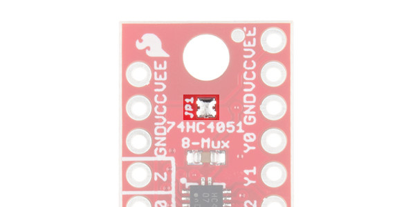
By connecting VEE to GND, you can satisfy both VCC-GND and VCC-VEE limits by keeping VCC between 2.0 and 10.0V. Unless you need a bipolar supply, you can leave this jumper closed and ignore VEE entirely.
Using a Bipolar Power Supply
The 74HC4051 supports bi-polar power supplies, with a positive supply on VCC and a negative supply on VEE. The difference between VCC and VEE can be as much as 10V (e.g. ±5V), but VCC must be somewhere between 2V and 10V.
To use a bipolar supply, you must first open JP1, disconnecting VEE from GND.

A quick hit of a soldering iron on some solder wick should lift that solder right up.
Once the jumper is open, your supplies can be connected. The logic levels of the select and enable pins will still be limited by VCC, but your common pin and eight I/O pins will be able to range between VEE and VCC.
Board Assembly
There is no one correct way to assemble the breakout, but you do need to solder something to the supply, select, common, and I/O pins. We recommend either male or female headers, but wire may be better suited to some projects.


The Multiplexer Breakout is breadboard-compatible, as the two header rows can span a breadboard’s inner trough. If you throw male headers onto the board…

…you can plug it in, and use jumper wires to connect the mux to an Arduino.

Arduino Example: Output
Now that you’ve got a handle on how to use the Multiplexer works and have the board assembled, here are a few quick example Arduino sketches to help demonstrate both output and input capabilities of the chip.
The Circuit
To get the most out of this example, you’ll need to connect some sort of output device to each of the independent I/O pins (Y0-Y7). For example, grab a pack of LEDs and some 330Ω resistors for a quick hardware-verifying circuit.

In this example, S0, S1, and S2 are connected to Arduino pins 2, 3 and 4 respectively. “Z” is connected to pin 5, which the example uses to produce PWM “analog output” signals.
VCC is connected to the Arduino 5V pin, and GND goes to GND. The breakout board’s JP1 is left intact, shorting VEE to GND.
Finally, the Y0-Y7 pins are all connected to LED/resistor pairs, with the positive anode end of the LED connected to the Y-pin and the resistor connecting the LED’s cathode to ground. This way, when the output is selected and “Z” goes high, the LED on that output will turn on.
The Sketch
Here’s the code for the above circuit. Upload it, and enjoy the cycling, breathing LEDs!
NOTE: For these examples, we're hosting the code on codebender, which not only features code-sharing, but also allows anyone to upload and debug Arduino sketches from within a web browser. Plus, it works on lower-tech machines, like Chromebooks!
There are codebender plugins for Chrome, Chromium, and Firefox. Visit the codebender plugin page for help installing the codebender plugin.
The magic part of this code is the selectMuxPin(byte pin) function at the bottom.
language:c
const int selectPins[3] = {2, 3, 4}; // S-pins to Arduino pins: S0~2, S1~3, S2~4
...
// The selectMuxPin function sets the S0, S1, and S2 pins to select the give pin
void selectMuxPin(byte pin)
{
  if (pin > 7) return; // Exit if pin is out of scope
  for (int i=0; i<3; i++)
  {
    if (pin & (1<<i))
      digitalWrite(selectPins[i], HIGH);
    else
      digitalWrite(selectPins[i], LOW);
  }
}
Given a pin number between 0 and 7, selectMuxPin configures the S0-S2 pins to connect that Y-pin to Z. If you take nothing else from this example, that function may prove the most handy in your future multiplexing endeavors.
Arduino Example: Input
In this example, we’ll switch gears and test out the 74HC4051’s analog signal support. By connecting “Z” to an analog input on the Arduino, we can turn one ADC pin into eight!
The Circuit
You can leave the select pins (S0-S2) tied to Arduino pins 2, 3, and 4, but re-route the Z jumper wire to A0. As for the Y-pins, you can connect potentiometers, photocells, or create voltage dividers on all eight inputs.

Connect the Multiplexer Breakout up to eight photocells to create a single-octave, touchless keyboard!
In lieu of a collection of eight analog input devices, you can just use jumper wires to short the input pins to either VCC or GND. That way you can at least prove to yourself that it works.
The Sketch
Here’s the sketch for the above circuit:
After uploading the sketch, open your serial monitor and set the baud rate to 9600. Here you’ll see the analog values from all eight independent I/O (Y0-Y7) read and printed out once a second.

Toggle your inputs, or switch out some jumper wires to see the values change.
This example uses that same selectMuxPin function to set the S0, S1, and S2 pins. But instead of writing out to the Z pin, we read from it.
Resources & Going Further
Need more information on the Multiplexer Breakout? There’s plenty where that came from! The 74HC4051’s datasheet is thorough and the breakout design is open-source:
- 74HC4051 Datasheet
- SparkFun Multiplexer Breakout Schematic
- SparkFun Multiplexer Breakout GitHub Repository
Or, if you need some inspiration in choosing your next project, check out some of these related tutorials:
Recreating Classic Electronics Kits
LogicBlocks Experiment Guide
learn.sparkfun.com |CC BY-SA 3.0 | SparkFun Electronics | Niwot, Colorado