Quantcast
Channel: SparkFun Tutorials
Viewing all 1123 articles
Browse latest View live

T5403 Barometric Pressure Sensor Hookup Guide

$
0
0

T5403 Barometric Pressure Sensor Hookup Guide a learn.sparkfun.com tutorial

Available online at: http://sfe.io/t205

Introduction

T5403 Breakout Board

The T5403 is a barometric pressure sensor with an I2C (“Wire”) interface.

Barometric pressure sensors measure the absolute pressure of the air around them. This pressure varies with both the weather and altitude. Depending on how you interpret the data, you can monitor changes in the weather, measure altitude, or any other tasks that require an accurate pressure reading.

Covered in This Tutorial

We will show you how to connect this sensor to an Arduino microcontroller and use the included software library to get measurements out of the sensor. We’ll also show you how to interpret the readings for both monitoring the weather and showing changes in altitude.

Suggested Reading

This part is easy to use. But before you start, we recommend the following background knowledge:

Connecting the Hardware

In this example, we will communicate with the T5403 using the I2C interface. While there are connections for SPI, they are currently unsupported.

Connection Names

The T5403 Breakout Board breaks out eight connections from the IC. We traditionally call these connections “pins” because they come from the pins on the IC, but they are actually holes that you can solder wires or header pins to.

T5403 breakout board

We’ll connect four of the eight pins on the board to your Arduino. The four pins you need are labeled GND, VCC, SCL, and SDA.

Connecting Wires to the Board

You can use any method you like to make your connections to the board. For this example, we’ll solder on a eight-pin length of male-male header strip, and use male-female jumper wires to connect the T5403 to your Arduino.

Solder a 8-pin length of male-male header to the board. You can solder it to either side. The bottom is more useful for breadboards, and the top is more useful for jumper wires.

T5403 Sensor with Headers

Note that the T5403 is sensitive to moisture. When you’re done soldering, do not clean off the flux by rinsing the board in water or other fluids.

Connecting the Board to your Arduino

When you’re done soldering, connect the +, -, CL, and DA pins to your Arduino. Different Arduino models use different pins for the I2C interface; use the following chart to determine where to plug everything in.

IMPORTANT: Connect the power pins (+ and -) ONLY to a 3.3V supply. Larger voltages will permanently damage the part. Note that because I2C uses open drain drivers, it is safe to connect the I2C pins (DA and CL) to an I2C port on a 5V microprocessor.

T5403 labelPin functionArduino connection
"-" (GND)groundGND
"+" (VDD)3.3V power supply3.3V
SDAI2C data Any pin labeled SDA, or:
Uno, Redboard, Pro / Pro MiniA4
Mega, Due20
Leonardo, Pro Micro2
SCLI2C clock Any pin labeled SCL, or:
Uno, Redboard, Pro / Pro MiniA5
Mega, Due21
Leonardo, Pro Micro3
MISOUnsupportedUnsupported
Reset/&SSDevice ResetAny I/O - Logic "LOW" to reset
SELI2C/SPI mode selectAny I/O - Logic "LOW" for SPI mode (Unsupported)
EOCEnd Of Conversion InterruptAny I/O or interrupt enabled pin - Outputs "HIGH" when measurement is complete

T5403 Frtizing Diagram

Once you have the T5403 connected to your Arduino, we’re ready to play with the software.

Installing the Arduino Library

Libraries are collections of software functions geared towards a single purpose, such as communicating with a specific device. Arduino comes with a number of built-in libraries that help you do advanced tasks. We’ve written an Arduino library called SFE_T5403 that allows you to easily talk to the T5403 sensor. This library is not included with the stock Arduino software, but don’t worry, installing new libraries is easy.

If you’d like to interface the T5403 to a microcontroller other than an Arduino, the C++ source code in the library and the information in the datasheet may be helpful when writing your own code.

1. Install the Arduino IDE

If you don’t already have the Arduino IDE (Integrated Development Environment) installed, download the version for your system (Windows, Mac, Linux) from http://arduino.cc/en/Main/Software and install it following the instructions on that site.

If you need help installing the IDE, check out our tutorial.

2. Install the SFE_T5403 Library

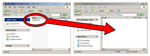
User-installed libraries live in a “libraries” folder within your personal Arduino sketch folder. On Windows systems your personal sketch folder is located in “My Documents/Arduino”. On Mac computers, it’s “~/Documents/Arduino”. On Linux it is usually “~/Arduino/sketchbook”. Locate your personal Arduino sketch folder and open it so you can drag new files into it.

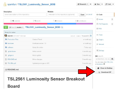
Now download the latest T5403 software archive from this link: https://github.com/sparkfun/T5403_Barometric_Breakout/archive/master.zip. You can either save the file to your system and open it later, or open it directly.

(Note that you can find the .zip file for any Github repository by looking for the “Download ZIP” button on the main page:)

alt text

Open the .zip file you just downloaded. (On most systems you should be able to double-click it to show the included files.) Open the folder called “T5403_Barometric_Breakout-master”, then “software”, then “Arduino”. You should now see a folder called “libraries”. Drag the “libraries” folder from the .zip folder into your personal Arduino sketch folder. If you get a warning that there is already a libraries folder there, that’s fine. It just means you’ve already installed some libraries, which is great! Just tell your system to go ahead and overwrite them, which sounds alarming but will only add the new library to the existing folder.

alt text

That’s it! Now restart the Arduino IDE and you should be ready to go.

If any of these instructions are unclear, you can find more detailed instructions in our installing an arduino library tutorial.

Running the Example Sketches

Running the Example Sketch

The library you just installed includes an example sketch that show basic operation of the T5403. This are designed to be a starting point for writing your own code.

After you install the library, run the Arduino IDE, and open the following menu item: File / Examples / SFE_T5403 / SFE_T5403_example.

(If you don’t see this menu item, you may not have installed the library correctly, or didn’t restart the Arduino IDE. Take another look at the library installation page to see if you missed any steps.)

alt text

When the example opens, upload it to your Arduino (remember to select the correct board type and serial port), and open the Serial Monitor to 9600 baud. You should see some diagnostic information (if it can’t find the device, double check your hardware connections) followed by measurement readings. For more about interpreting these readings, see the next page, Measuring Weather and Altitude.

Writing Your Own Sketches

The comments and code in the example sketch should get you started when writing your own sketches. In many cases you should be able to copy and paste the example code into your own sketch.

Measuring Weather and Altitude

The T5403 was designed to accurately measure atmospheric pressure. Atmospheric pressure varies with both weather and altitude; you can measure both of these using this sensor. Here’s how:

What is Atmospheric Pressure?

The definition of pressure is a force “pressing” on an area. A common unit of pressure is pounds per square inch (psi). One pound, pressing on one square inch, equals one psi. The SI unit is newtons per square meter, which are called pascals (Pa).

There are lots of situations in which pressure can be measured (gravity, pull, etc.), but right now we’re interested in atmospheric pressure, which is the force that the air around you is exerting on everything. The weight of the gases in the atmosphere creates atmospheric pressure. One doesn’t normally notice that air weighs anything, but if you took a one inch wide column of air from sea level to the top of the atmosphere, it would weigh about 14.7 pounds. (A 1 cm wide column of air would weigh about 1 kg.) This weight, pressing down on the footprint of that column, creates the atmospheric pressure that we can measure with sensors like the T5403.

Because that inch-wide column of air weighs about 14.7 pounds, and is pressing on one square inch, it follows that the average sea level pressure is about 14.7 pounds per square inch (psi), or 101325 pascals. This will drop about 4% for each 1000 feet (or 300 meters) you ascend. The higher you get, the less pressure you’ll see, because the column to the top of the atmosphere is that much shorter and therefore weighs less. This is useful to know, because by measuring the pressure and doing some math, you can determine your altitude.

Fun fact: The air pressure at 12,500 feet (3810 meters) is only half of that at sea level. In other words, half of the mass of the atmosphere is below 12,500 feet, and the air at 12,500 feet is half as dense as that at sea level. No wonder you have a harder time breathing up there.

The T5403 outputs absolute pressure in hectopascal (hPa). This is equivalent to 100 pascals (Pa). One pascal is a very small amount of pressure, approximately the amount that a sheet of paper will exert resting on a table. You will more often see measurements in hectopascals (1 hPa = 100 Pa) or kilopascals (1 kPa = 1000 Pa). The Arduino library we’ve provided outputs values in hPa, which also happens to equal one millibar (mbar).

Here are some conversions to other pressure units:

1 hPa = 100 Pa = 1 mbar = 0.001 bar

1 hPa = 0.75006168 Torr

1 hPa = 0.01450377 psi (pounds per square inch)

1 hPa = 0.02953337 inHg (inches of mercury)

1 hpa = 0.00098692 atm (standard atmospheres)

Temperature Effects

Because temperature affects the density of a gas, and density affects the mass of a gas, and mass affects the pressure (whew), atmospheric pressure will change dramatically with temperature. Pilots know this as “density altitude”, which makes it easier to take off on a cold day than a hot one because the air is more dense and has a greater aerodynamic effect.

To compensate for temperature, the T5403 includes a rather good temperature sensor as well as a pressure sensor. To perform a pressure reading, you first take a temperature reading, then combine that with a raw pressure reading to come up with a final temperature-compensated pressure measurement. (Don’t worry, the Arduino library makes all of this very easy.)

Measuring Absolute Pressure

As we just mentioned, if your application requires measuring absolute pressure, all you have to do is get a temperature reading, then perform a pressure reading (see the example sketch for details). The final pressure reading will be in hPa = mbar. If you wish, you can convert this to a different unit using the above conversion factors.

Note that the absolute pressure of the atmosphere will vary with both your altitude and the current weather patterns, both of which are useful things to measure.

Weather Observations

The atmospheric pressure at any given location on earth (or anywhere with an atmosphere) isn’t constant. The complex interaction between the earth’s spin, axis tilt, and many other factors result in moving areas of higher and lower pressure, which in turn cause the variations in weather we see every day. By watching for changes in pressure, you can predict short-term changes in the weather. For example, dropping pressure usually means wet weather or a storm is approaching (a low-pressure system is moving in). Rising pressure usually means that clear weather is approaching (a high-pressure system is moving through).

But remember that atmospheric pressure also varies with altitude. The absolute pressure in Denver (altitude 5280') will always be lower than the absolute pressure in San Francisco (altitude 52'). If weather stations just reported their absolute pressure, it would be difficult to directly compare pressure measurements from one location to another (and large-scale weather predictions depend on measurements from as many stations as possible).

To solve this problem, weather stations always remove the effects of altitude from their reported pressure readings by mathematically adding the equivalent fixed pressure to make it appear as if the reading was taken at sea level. When you do this, a higher reading in San Francisco than Denver will always be because of weather patterns, and not because of altitude.

To do this, there is a function in the sketch called seaLevel(P,A). This takes absolute pressure (P) in hPa, and the station’s current altitude (A) in meters, and removes the effects of the altitude from the pressure. You can use the output of this function to directly compare your weather readings to other stations around the world.

For more information, here is a good Wikipedia article on mean sea level pressure.

Determining Altitude

Since pressure varies with altitude, you can use a pressure sensor to measure altitude (with a few caveats).

The average pressure of the atmosphere at sea level is 1013.25 hPa (or mbar). This drops off to zero as you climb towards the vacuum of space. Because the curve of this drop-off is well understood, you can compute the altitude difference between two pressure measurements (p and p0) by using this equation:

alt text

There are two ways you can take advantage of this.

  1. If you use sea level pressure (1013.25 hPa) as the baseline pressure (p0), the output of the equation will be your current altitude above sea level.

  2. Or, if you take a single pressure reading at your current location, and use that as your baseline (p0), all subsequent pressure readings will result in relative altitude changes from the baseline. Climb the stairs and you should see the altitude go from zero to 3 or 4 meters. Go down to the basement, and you’ll see -3 or -4 meters. There’s an example function in the example sketch called altitude(P,P0) that calculates the relative altitude change. If you give it the sea level pressure (1013.25 hPa) for p0, and your local pressure for p, it will give you your altitude above sea level. If you use a local pressure measurement for p0, subsequent p pressure readings will give you your change in altitude from the baseline.

Now for the caveats:

Accuracy: How accurate is this? The theoretical noise level at the T5403s highest resolution is 0.25m (about 10 inches), though in practice we see noise on the order of 1m (40 inches). You can improve the accuracy by taking a large number of readings and averaging them, although this will slow down your sample rate and response time.

Weather: You should also remember that pressure changes due to weather will affect your altitude readings. The best accuracy will be obtained if you take a “fresh” p0 when you need it and don’t rely on it to be accurate for extended periods due to changes in the weather.

Maximum altitude: The T5403 can’t measure all the way down to vacuum (or up to space). It’s advertised lower limit is about 300 hPa (or mbar), which corresponds to an altitude of about 3000m or 30,000 feet. People have flown these to higher altitudes and gotten useful results, but this isn’t guaranteed or likely to be accurate. (You might consider using GPS for high-altitude measurements).

Minimum altitude: Similarly, this sensor isn’t suited for large pressures either. The advertised upper limit is 1100 hPa=mbar (or 16 psi), which is about 500 feet below sea level (that’s in air - the T5403 isn’t submersible in water). This sensor isn’t a good choice for submersible or compressed-gas measurements.

Tips and Tricks

Things to Watch Out For

Give it the right voltage: The T5403 will operate on voltages from 1.7v to 3.6v. We recommend operating it at 3.3V. Never connect the “+” header to voltages higher than 3.6V!. Note that it is safe to connect the SCA and SDL pins to an I2C port on a 5V Arduino, as the pullup resistors on the T5403 board will keep the voltage below 3.6V.

Give it air: Remember that the T5403 needs access to ambient air to measure its pressure, so don’t put it in a sealed case. Providing a small vent hole should be adequate.

But not too much air: On the other hand, exposure to fast-moving air or wind can cause momentary pressure variations that will affect your readings. Shield the device from strong air currents.

Keep it cool: Because an accurate temperature reading is needed to measure the pressure, try not to expose the device to rapid temperature changes, and keep it away from nearby hot parts and other heat sources.

Keep it dry: The T5403 is sensitive to moisture. Don’t submerge it or allow it to contact liquid water.

Changing the Solder Jumper

Solder jumpers are closely-spaced pads on a printed circuit board that are covered by blobs of solder to create an electrical connection. The T5403 breakout board has one such jumper; you can remove the solder from these pads to break the connection and alter the function of the board.

To remove the solder from a solder jumper, cover it with solder wick, and carefully heat it with a soldering iron. When the solder melts, it will be absorbed by the wick. Remove the wick before the solder cools so it doesn’t stick to the pads. If you didn’t get all of the solder on the first pass, give it another try with a clean section of solder wick. When you’re done you should be able to see a broken connection between the pads. While doing this be careful not to overheat the board (let it cool off if you’re having problems), or the copper pads may lift from the board.

T5403 Breakout Board

Disabling the I2C pullup resistors (SJ1)

The T5403 communicates with a host microcontroller via a communications standard called “I2C” (for Inter Integrated Circut). I2C uses two wires, usually labeled SCL (Serial Clock) and SDA (Serial Data). To function properly, I2C requires a pullup resistor on each of those lines. The T5403 board includes these resistors. They’re enabled by default, but you can disable them by clearing solder jumper.

I2C allows you to have multiple devices connected to the same two lines (collectively called a bus). The pullup resistors allow the bus to function, but you should only have one set of pullup resistors per bus.

If you have just one I2C device (such as the T5403 breakout board) connected to your microcontroller, the board is already set up properly. You don’t need to change anything.

However, if you wish to connect more than one device to the bus, you should ensure that there is only one set of pullup resistors enabled on the bus. You do this by disabling every set of pullup resistors except one. (It doesn’t matter where the enabled resistors live; they can be anywhere on the bus.)

To disable the I2C pullup resistors, remove all of the solder from the jumper. This jumper has three pads; be sure to separate all of the pads from each other. Remember that you’ll need to ensure that another set of pullup resistors are enabled somewhere on the I2C bus.

Note that you should not operate an I2C bus without pullup resistors, as the internal weak pull-up resistors in the Arduino will pull the bus to 5V, which may damage the T5403.

Using the EOC pin

The End of Conversion (EOC) pin is used to signal when the T5403 is finished taking a measurement. There is a waiting period to read a measurement from the device. This time varies with the measurement type and accuracy desired. The example code uses preset delays as stated in the data sheet.

Resources and Going Further

The example sketch included with the library should help you write your own code for the T5403. The code is commented to help you understand what it’s doing. In many cases, you should be able to copy and paste the example code into your own sketches. You may also want to refer to the datasheet and app note for more information about the internal workings of the sensor.

If you have any problems or questions, our technical support department can help. Please don’t hesitate to contact us. We also love to hear about your projects!

Further reading and projects:


learn.sparkfun.com |CC BY-SA 3.0 | SparkFun Electronics | Boulder, Colorado


Bubble Display Hookup Guide

$
0
0

Bubble Display Hookup Guide a learn.sparkfun.com tutorial

Available online at: http://sfe.io/t164

Introduction

The Bubble Display is a tiny 4-digit, 7-segment display. It’s perfect if you need some user feedback from your system, but don’t want to fiddle with LCDs or other display options. The Bubble Display comes in an easy-to-use DIP package and can be used in breadboards, protoboards, or PCBs.

bubble display

Covered in This Tutorial

This tutorial will go over the basic hardware requirements for the bubble display, show you how to hook one up to an Arduino microcontroller, and then show you a few different example sketches.

Required Materials

To follow along with all of the examples in this tutorial, you will need the following parts:


Suggested Reading

Before you go any further, check the tutorials below, and makes sure you have a good understanding of the concepts mentioned.

Hardware Overview

Let’s briefly discuss the characteristics and functionality of the bubble display before we connect it to other hardware.

All the information found on this page and more can be found in the product’s datasheet. Consult it, if you need more information.

Power

The bubble display is unique in that, unlike most ICs, these displays don’t need a supply voltage. The bubble display is four, 7-segment displays packed into one package, and 7-segment displays are really just seven LEDs lined up in a particular pattern. In this case, the number ‘8’ shape we’re all familiar with. Thus, to turn on and off a particular part of the display, you send it a digital HIGH or LOW signal just like you would with a regular LED.

However, you may have noticed that there are more LEDs than there are pins on the IC. There are 32 segments total (counting the decimal points) and only 12 pins. What gives? The answer is that these displays use common-cathode LEDs, which means all the LEDs in a given segment share one ground pin. This is the same method used in RGB LEDs that allows you to control three different colored LEDs with only four pins. With these displays, there are eight pins for the anodes (+) (seven segments and one decimal point per digit) and four pins for the cathode (-) of each digit.

alt text

A closeup of the bubble display.

With that said, you still want to limit the amount of current flowing through the LEDs. If you are using a 5V microcontroller such as a SparkFun RedBoard, you’ll need to add current limiting resistors to your circuit. Even if you’re using a 3.3V micro, you should still add resistors, albeit much smaller values. The following tables from the datasheet give us the information we need to calculate the correct resistor value.

alt text

LED calculators, such as this one make it easy to figure out which value resistor to use. For example, if you’re using a 5V source to control the segments, you’ll want to have a 680 Ω resistor in line with each, assuming that each segment is operating under normal conditions. If you find that the display isn’t as bright as you’d like it, you can always add a smaller value resistor. We’ve found that a 330Ω resistor works well on all four cathode pins.

Pinout

Now that we know how to properly provide power to the display, let’s go over the segment configuration so we know which pins light up which segments. The pinout for the bubble display is as follows.

pinout table

Next, take a look at the segment key.

alt text

Last, here is a diagram showing the numbering of the digits as they correspond to the pins labeled above.

alt text

Don’t forget that most ICs are polarized. Pin 1 is indicated by the small dot on the underside of the board.

Building from what we discussed above, we can start to make sense of this. For example, let’s say we wanted to turn on Segment_A on Digit_1. Looking at the table above we see that Segment_A (labeled Anode a) is pin 12. Looking at the same table, we can also see that the cathode for Digit_1 is pin 1. If you connect pin 1 to GND, and pin 12 to 3.3V or 5V (don’t forget that resistor!), you should see the topmost segment on the leftmost digit light up. Yay LEDs! From here you can extrapolate how the rest works. If you wanted to light up Segment_A on both Digit_1 and Digit_4, you would simply add another connection to our first example from GND to pin 6 (cathode 4), and so on…


Lighting up individual segments is fun for about a minute, so let’s move on and get this thing displaying some useful information.

Hooking it Up

In order to talk to the bubble display, we’ll need a microcontroller. This example will use a SparkFun RedBoard to control the display, but you can use whichever you choose. You’ll also need some jumper wires, some resistors, and a breadboard.

This IC is polarized, so pay attention to which way you stick it in the breadboard! Pin one is indicated by a white dot on the underside of the part.

alt text

Once you have the bubble display oriented correctly on the breadboard, hook everything up like the image below shows:

alt text

Note the polarity mark on the bottom-left corner of the bubble display. Click the image for a larger view.

While the display may work without current limiting resistors, it’s always a good idea to have them in your circuit to avoid burning out your display. Instead of individual resistors, you could also use one of these resistor networks.


Now, it’s time to light up the display with some code.

Firmware

Before you can start writing code to control the bubble displays, you’ll need to install the SevSeg Arduino Library first. You can download it from the GitHub repo. If you need more details on installing a library, visit our Installing an Arduino Library tutorial, and, if you are unfamiliar with GitHub, there’s a tutorial for that too.

Once the library is installed, we can use the included example sketches to get started using the bubble display.

Example 1: Counter

Go to File -> Examples -> SevSeg -> Example -> Bubble_Display_Counter.

Here is the code for those who would like to see it without downloading it.

language:c
/*
 March 6, 2014
 Spark Fun Electronics
 Nathan Seidle
 Updates by Joel Bartlett

 This code is originally based Dean Reading's Library deanreading@hotmail.com
 http://arduino.cc/playground/Main/SevenSegmentLibrary
 He didn't have a license on it so I hope he doesn't mind me making it public domain:
 This code is public domain but you buy me a beer if you use this and we meet someday (Beerware license).

 This sketch provides a simple counter example for the HP Bubble display from SparkFun.
 https://www.sparkfun.com/products/12710

 Pinout for HP Bubble Display:
 1:  Cathode 1
 2:  Anode E
 3:  Anode C
 4:  Cathode 3
 5:  Anode dp
 6:  Cathode 4
 7:  Anode G
 8:  Anode D
 9:  Anode F
 10: Cathode 2
 11: Anode B
 12: Anode A
 */

#include "SevSeg.h"

//Create an instance of the object.
SevSeg myDisplay;

//Create global variables
unsigned long timer;
int deciSecond = 0;

void setup()
{

  int displayType = COMMON_CATHODE; //Your display is either common cathode or common anode


  //This pinout is for a bubble dispaly
   //Declare what pins are connected to the digits
   int digit1 = 8; //Pin 12 on my 4 digit display
   int digit2 = 5; //Pin 9 on my 4 digit display
   int digit3 = 11; //Pin 8 on my 4 digit display
   int digit4 = 13; //Pin 6 on my 4 digit display

   //Declare what pins are connected to the segments
   int segA = 7; //Pin 11 on my 4 digit display
   int segB = 6; //Pin 7 on my 4 digit display
   int segC = 10; //Pin 4 on my 4 digit display
   int segD = 3; //Pin 2 on my 4 digit display
   int segE = 9; //Pin 1 on my 4 digit display
   int segF = 4; //Pin 10 on my 4 digit display
   int segG = 2; //Pin 5 on my 4 digit display
   int segDP= 12; //Pin 3 on my 4 digit display

  int numberOfDigits = 4; //Do you have a 1, 2 or 4 digit display?

  myDisplay.Begin(displayType, numberOfDigits, digit1, digit2, digit3, digit4, segA, segB, segC, segD, segE, segF, segG, segDP);

  myDisplay.SetBrightness(100); //Set the display to 100% brightness level

  timer = millis();
}

void loop()
{
  //Example ways of displaying a decimal number
  char tempString[10]; //Used for sprintf
  sprintf(tempString, "%4d", deciSecond); //Convert deciSecond into a string that is right adjusted
  //sprintf(tempString, "%d", deciSecond); //Convert deciSecond into a string that is left adjusted
  //sprintf(tempString, "%04d", deciSecond); //Convert deciSecond into a string with leading zeros
  //sprintf(tempString, "%4d", deciSecond * -1); //Shows a negative sign infront of right adjusted number
  //sprintf(tempString, "%4X", deciSecond); //Count in HEX, right adjusted

  //Produce an output on the display
  myDisplay.DisplayString(tempString, 0); //(numberToDisplay, decimal point location)

  //Other examples
  //myDisplay.DisplayString(tempString, 0); //Display string, no decimal point
  //myDisplay.DisplayString("-23b", 3); //Display string, decimal point in third position

  //Check if 10ms has elapsed
  if (millis() - timer >= 100)
  {
    timer = millis();
    deciSecond++;
  }

  delay(5);
}

With this sketch uploaded, the display with count up, with each order of magnitude spilling onto the next digit to the left.

Example 2: Text

The next example shows how to display text. Since these display are 7-segment and not alphanumeric, they are limited in which characters they can and can’t display. The sketch has a table listing all there characters and whether or not they can be displayed.

To open this sketch, go to File -> Examples -> SevSeg -> Example -> Bubble_Display_Text.

language:c
/*
 March 6, 2014
 Spark Fun Electronics
 Nathan Seidle
 Updates by Joel Bartlett

 This code is originally based Dean Reading's Library deanreading@hotmail.com
 http://arduino.cc/playground/Main/SevenSegmentLibrary
 He didn't have a license on it so I hope he doesn't mind me making it public domain:
 This code is public domain but you buy me a beer if you use this and we meet someday (Beerware license).

The example shows you how to display characters to the bubble display. Since this is a 7-segment display
and not an alpha-numeric display, there are numerous characters that cannot be displayed. The table below
should give you an idea which ones can.


 Pinout for HP Bubble Display:
 1:  Cathode 1
 2:  Anode E
 3:  Anode C
 4:  Cathode 3
 5:  Anode dp
 6:  Cathode 4
 7:  Anode G
 8:  Anode D
 9:  Anode F
 10: Cathode 2
 11: Anode B
 12: Anode A

 Here is the character map found in the SevSeg.h file for reference
 as to which characters can be displayed and which can't.

 //  ABCDEFG  Segments
  0b1111110, // 0
  0b0110000, // 1
  0b1101101, // 2
  0b1111001, // 3
  0b0110011, // 4
  0b1011011, // 5
  0b1011111, // 6
  0b1110000, // 7
  0b1111111, // 8
  0b1111011, // 9
  0b1110111, // 10  "A"
  0b0011111, // 11  "B"
  0b1001110, // 12  "C"
  0b0111101, // 13  "D"
  0b1001111, // 14  "E"
  0b1000111, // 15  "F"
  0b0000000, // 16  NO DISPLAY
  0b0000000, // 17  NO DISPLAY
  0b0000000, // 18  NO DISPLAY
  0b0000000, // 19  NO DISPLAY
  0b0000000, // 20  NO DISPLAY
  0b0000000, // 21  NO DISPLAY
  0b0000000, // 22  NO DISPLAY
  0b0000000, // 23  NO DISPLAY
  0b0000000, // 24  NO DISPLAY
  0b0000000, // 25  NO DISPLAY
  0b0000000, // 26  NO DISPLAY
  0b0000000, // 27  NO DISPLAY
  0b0000000, // 28  NO DISPLAY
  0b0000000, // 29  NO DISPLAY
  0b0000000, // 30  NO DISPLAY
  0b0000000, // 31  NO DISPLAY
  0b0000000, // 32 ' '
  0b0000000, // 33 '!'  NO DISPLAY
  0b0100010, // 34 '"'
  0b0000000, // 35 '#'  NO DISPLAY
  0b0000000, // 36 '$'  NO DISPLAY
  0b0000000, // 37 '%'  NO DISPLAY
  0b0000000, // 38 '&'  NO DISPLAY
  0b0100000, // 39 '''
  0b1001110, // 40 '('
  0b1111000, // 41 ')'
  0b0000000, // 42 '*'  NO DISPLAY
  0b0000000, // 43 '+'  NO DISPLAY
  0b0000100, // 44 ','
  0b0000001, // 45 '-'
  0b0000000, // 46 '.'  NO DISPLAY
  0b0000000, // 47 '/'  NO DISPLAY
  0b1111110, // 48 '0'
  0b0110000, // 49 '1'
  0b1101101, // 50 '2'
  0b1111001, // 51 '3'
  0b0110011, // 52 '4'
  0b1011011, // 53 '5'
  0b1011111, // 54 '6'
  0b1110000, // 55 '7'
  0b1111111, // 56 '8'
  0b1111011, // 57 '9'
  0b0000000, // 58 ':'  NO DISPLAY
  0b0000000, // 59 ';'  NO DISPLAY
  0b0000000, // 60 '<'  NO DISPLAY
  0b0000000, // 61 '='  NO DISPLAY
  0b0000000, // 62 '>'  NO DISPLAY
  0b0000000, // 63 '?'  NO DISPLAY
  0b0000000, // 64 '@'  NO DISPLAY
  0b1110111, // 65 'A'
  0b0011111, // 66 'B'
  0b1001110, // 67 'C'
  0b0111101, // 68 'D'
  0b1001111, // 69 'E'
  0b1000111, // 70 'F'
  0b1011110, // 71 'G'
  0b0110111, // 72 'H'
  0b0110000, // 73 'I'
  0b0111000, // 74 'J'
  0b0000000, // 75 'K'  NO DISPLAY
  0b0001110, // 76 'L'
  0b0000000, // 77 'M'  NO DISPLAY
  0b0010101, // 78 'N'
  0b1111110, // 79 'O'
  0b1101111, // 80 'P'
  0b1110011, // 81 'Q'
  0b0000101, // 82 'R'
  0b1011011, // 83 'S'
  0b0001111, // 84 'T'
  0b0111110, // 85 'U'
  0b0000000, // 86 'V'  NO DISPLAY
  0b0000000, // 87 'W'  NO DISPLAY
  0b0000000, // 88 'X'  NO DISPLAY
  0b0111011, // 89 'Y'
  0b0000000, // 90 'Z'  NO DISPLAY
  0b1001110, // 91 '['
  0b0000000, // 92 '\'  NO DISPLAY
  0b1111000, // 93 ']'
  0b0000000, // 94 '^'  NO DISPLAY
  0b0001000, // 95 '_'
  0b0000010, // 96 '`'
  0b1110111, // 97 'a' SAME AS CAP
  0b0011111, // 98 'b' SAME AS CAP
  0b0001101, // 99 'c'
  0b0111101, // 100 'd' SAME AS CAP
  0b1101111, // 101 'e'
  0b1000111, // 102 'f' SAME AS CAP
  0b1011110, // 103 'g' SAME AS CAP
  0b0010111, // 104 'h'
  0b0010000, // 105 'i'
  0b0111000, // 106 'j' SAME AS CAP
  0b0000000, // 107 'k'  NO DISPLAY
  0b0110000, // 108 'l'
  0b0000000, // 109 'm'  NO DISPLAY
  0b0010101, // 110 'n' SAME AS CAP
  0b0011101, // 111 'o'
  0b1100111, // 112 'p' SAME AS CAP
  0b1110011, // 113 'q' SAME AS CAP
  0b0000101, // 114 'r' SAME AS CAP
  0b1011011, // 115 's' SAME AS CAP
  0b0001111, // 116 't' SAME AS CAP
  0b0011100, // 117 'u'
  0b0000000, // 118 'b'  NO DISPLAY
  0b0000000, // 119 'w'  NO DISPLAY
  0b0000000, // 120 'x'  NO DISPLAY
  0b0000000, // 121 'y'  NO DISPLAY
  0b0000000, // 122 'z'  NO DISPLAY
  0b0000000, // 123 '0b'  NO DISPLAY
  0b0000000, // 124 '|'  NO DISPLAY
  0b0000000, // 125 ','  NO DISPLAY
  0b0000000, // 126 '~'  NO DISPLAY
  0b0000000, // 127 'DEL'  NO DISPLAY
 */

#include "SevSeg.h"

//Create an instance of the object.
SevSeg myDisplay;

//Create global variables
unsigned long timer;
int deciSecond = 0;

void setup()
{

  int displayType = COMMON_CATHODE; //Your display is either common cathode or common anode


  //This pinout is for a bubble dispaly
   //Declare what pins are connected to the digits
   int digit1 = 8; //Pin 12 on my 4 digit display
   int digit2 = 5; //Pin 9 on my 4 digit display
   int digit3 = 11; //Pin 8 on my 4 digit display
   int digit4 = 13; //Pin 6 on my 4 digit display

   //Declare what pins are connected to the segments
   int segA = 7; //Pin 11 on my 4 digit display
   int segB = 6; //Pin 7 on my 4 digit display
   int segC = 10; //Pin 4 on my 4 digit display
   int segD = 3; //Pin 2 on my 4 digit display
   int segE = 9; //Pin 1 on my 4 digit display
   int segF = 4; //Pin 10 on my 4 digit display
   int segG = 2; //Pin 5 on my 4 digit display
   int segDP= 12; //Pin 3 on my 4 digit display

  int numberOfDigits = 4; //Do you have a 1, 2 or 4 digit display?

  myDisplay.Begin(displayType, numberOfDigits, digit1, digit2, digit3, digit4, segA, segB, segC, segD, segE, segF, segG, segDP);

  myDisplay.SetBrightness(100); //Set the display to 100% brightness level

  timer = millis();
}

void loop()
{
  char tempString[5] = {'C','O','D','E'}; //Used for sprintf

  for(int i =0;i<100;i++)
  {

  myDisplay.DisplayString(tempString, 0); //(numberToDisplay, decimal point location)

  delay(10);
  }

   for(int i =0;i<100;i++)
  {
      tempString[0] = 58;
      tempString[1] = 'I';
      tempString[2] = 'S';
      tempString[3] = 58;

      myDisplay.DisplayString(tempString, 0);

      delay(10);
  }
   for(int i =0;i<100;i++)
  {
      tempString[0] = 'C';
      tempString[1] = 'O';
      tempString[2] = 'O';
      tempString[3] = 'L';

      myDisplay.DisplayString(tempString, 0);

      delay(10);
  }

}

Example 3: Sensor Data

This last example is more of a real-world application. By adding a temperature and humidity sensor to the RedBoard, we can make a tiny, digital thermometer and hygrometer.

First, you need to add a SHT15 to your circuit. You may use whatever sensors you like, but you will need to alter the code accordingly.

alt text

Click for larger view.

Now, go to File -> Examples -> SevSeg -> Example -> Bubble_Display_SHT15 to open up the sketch.

language:c
/*
 March 6, 2014
 Spark Fun Electronics
 Nathan Seidle
 Updates by Joel Bartlett

 This code is originally based Dean Reading's Library deanreading@hotmail.com
 http://arduino.cc/playground/Main/SevenSegmentLibrary
 He didn't have a license on it so I hope he doesn't mind me making it public domain:
 This code is public domain but you buy me a beer if you use this and we meet someday (Beerware license).

This example gives you a real world scenario in which we take sensor data (in this case temperature and humidity
data from a SHT15) and print it to the bubble display using characters and numbers.


 Pinout for HP Bubble Display:
 1:  Cathode 1
 2:  Anode E
 3:  Anode C
 4:  Cathode 3
 5:  Anode dp
 6:  Cathode 4
 7:  Anode G
 8:  Anode D
 9:  Anode F
 10: Cathode 2
 11: Anode B
 12: Anode A

 Pinout for SHT15:
 Vcc: 3.3V
 Data: A4 or SDA on newer Arduino boards
 SCK: A5 or SCK on newer Arduino boards
 GND: GND

 Here is the character map found in the SevSeg.h file for reference
 as to which characters can be displayed and which can't.

 //  ABCDEFG  Segments
  0b1111110, // 0
  0b0110000, // 1
  0b1101101, // 2
  0b1111001, // 3
  0b0110011, // 4
  0b1011011, // 5
  0b1011111, // 6
  0b1110000, // 7
  0b1111111, // 8
  0b1111011, // 9
  0b1110111, // 10  "A"
  0b0011111, // 11  "B"
  0b1001110, // 12  "C"
  0b0111101, // 13  "D"
  0b1001111, // 14  "E"
  0b1000111, // 15  "F"
  0b0000000, // 16  NO DISPLAY
  0b0000000, // 17  NO DISPLAY
  0b0000000, // 18  NO DISPLAY
  0b0000000, // 19  NO DISPLAY
  0b0000000, // 20  NO DISPLAY
  0b0000000, // 21  NO DISPLAY
  0b0000000, // 22  NO DISPLAY
  0b0000000, // 23  NO DISPLAY
  0b0000000, // 24  NO DISPLAY
  0b0000000, // 25  NO DISPLAY
  0b0000000, // 26  NO DISPLAY
  0b0000000, // 27  NO DISPLAY
  0b0000000, // 28  NO DISPLAY
  0b0000000, // 29  NO DISPLAY
  0b0000000, // 30  NO DISPLAY
  0b0000000, // 31  NO DISPLAY
  0b0000000, // 32 ' '
  0b0000000, // 33 '!'  NO DISPLAY
  0b0100010, // 34 '"'
  0b0000000, // 35 '#'  NO DISPLAY
  0b0000000, // 36 '$'  NO DISPLAY
  0b0000000, // 37 '%'  NO DISPLAY
  0b0000000, // 38 '&'  NO DISPLAY
  0b0100000, // 39 '''
  0b1001110, // 40 '('
  0b1111000, // 41 ')'
  0b0000000, // 42 '*'  NO DISPLAY
  0b0000000, // 43 '+'  NO DISPLAY
  0b0000100, // 44 ','
  0b0000001, // 45 '-'
  0b0000000, // 46 '.'  NO DISPLAY
  0b0000000, // 47 '/'  NO DISPLAY
  0b1111110, // 48 '0'
  0b0110000, // 49 '1'
  0b1101101, // 50 '2'
  0b1111001, // 51 '3'
  0b0110011, // 52 '4'
  0b1011011, // 53 '5'
  0b1011111, // 54 '6'
  0b1110000, // 55 '7'
  0b1111111, // 56 '8'
  0b1111011, // 57 '9'
  0b0000000, // 58 ':'  NO DISPLAY
  0b0000000, // 59 ';'  NO DISPLAY
  0b0000000, // 60 '<'  NO DISPLAY
  0b0000000, // 61 '='  NO DISPLAY
  0b0000000, // 62 '>'  NO DISPLAY
  0b0000000, // 63 '?'  NO DISPLAY
  0b0000000, // 64 '@'  NO DISPLAY
  0b1110111, // 65 'A'
  0b0011111, // 66 'B'
  0b1001110, // 67 'C'
  0b0111101, // 68 'D'
  0b1001111, // 69 'E'
  0b1000111, // 70 'F'
  0b1011110, // 71 'G'
  0b0110111, // 72 'H'
  0b0110000, // 73 'I'
  0b0111000, // 74 'J'
  0b0000000, // 75 'K'  NO DISPLAY
  0b0001110, // 76 'L'
  0b0000000, // 77 'M'  NO DISPLAY
  0b0010101, // 78 'N'
  0b1111110, // 79 'O'
  0b1101111, // 80 'P'
  0b1110011, // 81 'Q'
  0b0000101, // 82 'R'
  0b1011011, // 83 'S'
  0b0001111, // 84 'T'
  0b0111110, // 85 'U'
  0b0000000, // 86 'V'  NO DISPLAY
  0b0000000, // 87 'W'  NO DISPLAY
  0b0000000, // 88 'X'  NO DISPLAY
  0b0111011, // 89 'Y'
  0b0000000, // 90 'Z'  NO DISPLAY
  0b1001110, // 91 '['
  0b0000000, // 92 '\'  NO DISPLAY
  0b1111000, // 93 ']'
  0b0000000, // 94 '^'  NO DISPLAY
  0b0001000, // 95 '_'
  0b0000010, // 96 '`'
  0b1110111, // 97 'a' SAME AS CAP
  0b0011111, // 98 'b' SAME AS CAP
  0b0001101, // 99 'c'
  0b0111101, // 100 'd' SAME AS CAP
  0b1101111, // 101 'e'
  0b1000111, // 102 'f' SAME AS CAP
  0b1011110, // 103 'g' SAME AS CAP
  0b0010111, // 104 'h'
  0b0010000, // 105 'i'
  0b0111000, // 106 'j' SAME AS CAP
  0b0000000, // 107 'k'  NO DISPLAY
  0b0110000, // 108 'l'
  0b0000000, // 109 'm'  NO DISPLAY
  0b0010101, // 110 'n' SAME AS CAP
  0b0011101, // 111 'o'
  0b1100111, // 112 'p' SAME AS CAP
  0b1110011, // 113 'q' SAME AS CAP
  0b0000101, // 114 'r' SAME AS CAP
  0b1011011, // 115 's' SAME AS CAP
  0b0001111, // 116 't' SAME AS CAP
  0b0011100, // 117 'u'
  0b0000000, // 118 'b'  NO DISPLAY
  0b0000000, // 119 'w'  NO DISPLAY
  0b0000000, // 120 'x'  NO DISPLAY
  0b0000000, // 121 'y'  NO DISPLAY
  0b0000000, // 122 'z'  NO DISPLAY
  0b0000000, // 123 '0b'  NO DISPLAY
  0b0000000, // 124 '|'  NO DISPLAY
  0b0000000, // 125 ','  NO DISPLAY
  0b0000000, // 126 '~'  NO DISPLAY
  0b0000000, // 127 'DEL'  NO DISPLAY

  SHT15 code based on the code found at Wiring.org
  http://wiring.org.co/learning/basics/humiditytemperaturesht15.html

 */


#include "SevSeg.h"

//Create an instance of the object.
SevSeg myDisplay;

int temperatureCommand  = B00000011;  // command used to read temperature
int humidityCommand = B00000101;  // command used to read humidity

int clockPin = A5;  // pin used for clock
int dataPin  = A4;  // pin used for data
int ack;  // track acknowledgment for errors
int val;
float tempF;
float humidity;
float tempC;

char tempString[5];
//-------------------------------------------------------------------------------------------
void setup()
{
 int displayType = COMMON_CATHODE; //Your display is either common cathode or common anode

  //This pinout is for a regular display
   //Declare what pins are connected to the digits
   int digit1 = 8; //Pin 12 on my 4 digit display
   int digit2 = 5; //Pin 9 on my 4 digit display
   int digit3 = 11; //Pin 8 on my 4 digit display
   int digit4 = 13; //Pin 6 on my 4 digit display

   //Declare what pins are connected to the segments
   int segA = 7; //Pin 11 on my 4 digit display
   int segB = 6; //Pin 7 on my 4 digit display
   int segC = 10; //Pin 4 on my 4 digit display
   int segD = 3; //Pin 2 on my 4 digit display
   int segE = 9; //Pin 1 on my 4 digit display
   int segF = 4; //Pin 10 on my 4 digit display
   int segG = 2; //Pin 5 on my 4 digit display
   int segDP= 12; //Pin 3 on my 4 digit display

  int numberOfDigits = 4; //Do you have a 1, 2 or 4 digit display?

  myDisplay.Begin(displayType, numberOfDigits, digit1, digit2, digit3, digit4, segA, segB, segC, segD, segE, segF, segG, segDP);

  myDisplay.SetBrightness(100); //Set the display to 100% brightness level
}
//-------------------------------------------------------------------------------------------
void loop()
{

  sht15();
  clear();
  for(int i =0;i<500;i++)
  {
      tempString[0] = 'T';
      tempString[1] = 'F';

      myDisplay.DisplayString(tempString, 0);

    sprintf(tempString, "%4d",  (long)tempF, DEC);
    myDisplay.DisplayString(tempString, 0);
  }
  clear();
   for(int i =0;i<500;i++)
  {
      tempString[0] = 'R';
      tempString[1] = 'H';

    myDisplay.DisplayString(tempString, 0);

    sprintf(tempString, "%4d",  (long)humidity, DEC);
    myDisplay.DisplayString(tempString, 0);
  }
}
//-------------------------------------------------------------------------------------------
void clear()
{
      //write a non-displayable character to each position to clear the display
      tempString[0] = 'm';
      tempString[1] = 'm';
      tempString[2] = 'm';
      tempString[3] = 'm';

      myDisplay.DisplayString(tempString, 0);
}
//-------------------------------------------------------------------------------------------
int sht15()
{
  // read the temperature and convert it to centigrades
  sendCommandSHT(temperatureCommand, dataPin, clockPin);
  waitForResultSHT(dataPin);
  val = getData16SHT(dataPin, clockPin);
  skipCrcSHT(dataPin, clockPin);
  tempC = (float)val * 0.01 - 40;
  tempF = (float)tempC * 1.8 + 32;

  //Serial.print("Temperature: ");
  //Serial.print((long)tempF, DEC);
  //Serial.print("_");
  //Serial.print((char)176);
  //Serial.print("F ");

  // read the humidity
  sendCommandSHT(humidityCommand, dataPin, clockPin);
  waitForResultSHT(dataPin);
  val = getData16SHT(dataPin, clockPin);
  skipCrcSHT(dataPin, clockPin);
  humidity = -4.0 + 0.0405 * val + -0.0000028 * val * val;

  //Serial.print(" Relative Humidity: ");
  //Serial.print((long)humidity, DEC);
   //Serial.println("%");
  //delay(1000); // wait for 3 sec for next reading
  return tempF, tempC, humidity;
}


// commands for reading/sending data to a SHTx sensor

int shiftIn(int dataPin, int clockPin, int numBits) {
  int ret = 0;

  for (int i=0; i<numBits; ++i) {
    digitalWrite(clockPin, HIGH);
    //delay(10); not needed :)
    ret = ret*2 + digitalRead(dataPin);
    digitalWrite(clockPin, LOW);
  }
  return(ret);
}

// send a command to the SHTx sensor
void sendCommandSHT(int command, int dataPin, int clockPin) {
  int ack;

  // transmission start
  pinMode(dataPin, OUTPUT);
  pinMode(clockPin, OUTPUT);
  digitalWrite(dataPin, HIGH);
  digitalWrite(clockPin, HIGH);
  digitalWrite(dataPin, LOW);
  digitalWrite(clockPin, LOW);
  digitalWrite(clockPin, HIGH);
  digitalWrite(dataPin, HIGH);
  digitalWrite(clockPin, LOW);

  // shift out the command (the 3 MSB are address and must be 000, the last 5 bits are the command)
  shiftOut(dataPin, clockPin, MSBFIRST, command);

  // verify we get the right ACK
  digitalWrite(clockPin, HIGH);
  pinMode(dataPin, INPUT);
  ack = digitalRead(dataPin);
  if (ack != LOW)
    Serial.println("ACK error 0");
  digitalWrite(clockPin, LOW);
  ack = digitalRead(dataPin);
  if (ack != HIGH)
    Serial.println("ACK error 1");
}

// wait for the SHTx answer
void waitForResultSHT(int dataPin) {
  int ack;

  pinMode(dataPin, INPUT);
  for(int i=0; i<100; ++i) {
    delay(10);
    ack = digitalRead(dataPin);
    if (ack == LOW)
      break;
  }
  if (ack == HIGH)
    Serial.println("ACK error 2");
}

// get data from the SHTx sensor
int getData16SHT(int dataPin, int clockPin) {
  int val;

  // get the MSB (most significant bits)
  pinMode(dataPin, INPUT);
  pinMode(clockPin, OUTPUT);
  val = shiftIn(dataPin, clockPin, 8);
  val *= 256; // this is equivalent to val << 8;

  // send the required ACK
  pinMode(dataPin, OUTPUT);
  digitalWrite(dataPin, HIGH);
  digitalWrite(dataPin, LOW);
  digitalWrite(clockPin, HIGH);
  digitalWrite(clockPin, LOW);

  // get the LSB (less significant bits)
  pinMode(dataPin, INPUT);
  val |= shiftIn(dataPin, clockPin, 8);
  return val;
}

// skip CRC data from the SHTx sensor
void skipCrcSHT(int dataPin, int clockPin) {
  pinMode(dataPin, OUTPUT);
  pinMode(clockPin, OUTPUT);
  digitalWrite(dataPin, HIGH);
  digitalWrite(clockPin, HIGH);
  digitalWrite(clockPin, LOW);
}
//-------------------------------------------------------------------------------------------

When you run the sketch, it should start off by printing tF followed by the temperature in fahrenheit. After ten seconds, it should display rH folowed by the current relative humidity. After ten more seconds the cycle will repeat.

alt text

Check out the New Product Showcase video to see the dispaly in action.

Resources and Going Further

For more information on the bubble display, be sure to read the datasheet.

For more great tutorials and 7-segment displays and LCDs, check out these other offerings from SparkFun Electronics:


learn.sparkfun.com |CC BY-SA 3.0 | SparkFun Electronics | Boulder, Colorado

HID Control of a Web Page

$
0
0

HID Control of a Web Page a learn.sparkfun.com tutorial

Available online at: http://sfe.io/t177

HID Communication

Moving data between a microcontroller and a computer is tricky. Up to this point the serial protocol and USB-to-Serial converters have filled the gap. Today we will show you how to listen to and control a USB HID based board via a webpage. This is very helpful if your designing an interactive webpage that needs to respond to the physical world.

Human Interface Devices, or HID, was created to allow lots of different types of hardware to pass information back and forth over USB. A keyboard is a good HID example but a keyboard only passes data in one direction (‘you pressed the k button’). Full duplex is more complicated but is much more valuable once you have it up and running.

Motor control from a webpage

It’s not pretty, but the sky is the limit when you can read and control hardware from a web page!

Covered in This Tutorial

This is not a ‘turn your Leonardo into a keyboard’ example. This tutorial demonstrates full two-way HID communication. This technique is helpful if you need to control outputs such as motors, LEDs, and buzzers. We apologize, but certain tools used in this tutorial are Windows only. If you have similar tool chains to get RawHID working on Linux and Mac please let us know.

This tutorial is based heavily on the Teensy RawHID library by PJRC. None of this would be possible without Paul’s awesome work developing the RawHID library. If you’re thinking about making a true USB device, consider developing it with a Teensy from PJRC or from SparkFun. They are truly easy-to-use little devices.

The idea behind this tutorial came from a project where we needed to create a board the could output sensor data (analog values, digital values) to a web page. We also needed to control motors and LEDs based on where the user clicked on that same page. To do this we needed the board to be able to pass HID packets back and forth. Again, there are plenty of tutorials out there showing how to implement a joystick or a keyboard, but these are often one way and rarely talk directly to a webpage.

Required Materials

Here’s a list of parts you may want to gather:

You can add all these parts to your cart then remove any you already have.

Suggested Reading/Viewing:

Teensy Setup

Teensy in a breadboard

Let’s start by having the Teensy report HID packets. At this point we only need to attach a USB cable to the Teensy.

To get use RawHID you’ll need to install Teensyduino. For help installing Teensyduino see the PJRC site.

RawHID Menu in Arduino

Once Teensyduino is installed, you’ll have access to the Raw HID USB type as well as a basic example sketch. Before we continue there are some settings that can be modified. Find the usb_private.h file located in the \Arduino\hardware\teensy\cores\usb_rawhid folder, and open it in a text editor. The usb_private file contains the VID/PID, device string, and frame settings when using the RawHID library.

Vendor ID / Product ID

If you’re just learning how to control HID there is no need to change the VID/PID settings. If you are rolling your own hardware you’ll need to tweak the vendor ID and product ID. Don’t have your own Vendor ID? That’s kind of a problem, but, if you’re just playing around, don’t worry about it too much. If you’re planning on selling 10,000 of your device then you’ll need to spend the $5,000 to get your own VID.

Device String

This is the human readable string that is commonly shown when the USB is plugged in. It may sound fun to attach the ‘NSA Webcam Controller’ to your friend’s computer, but let’s leave the STR_PRODUCT alone for now.

Frame Size

The frame size (RAWHID_TX_SIZE and RAWHID_RX_SIZE) is what you should focus on within usb_private.h. How much data do you need to pass back and forth? For this tutorial, we are going to show how to read up to eight, 16-bit sensors, so we define RAWHID_TX_SIZE to be 16 bytes. To make things symetrical, let’s set the size of the RAWHID_RX_SIZE to 16 bytes as well. These buffers can be any size (256 byte max), but try to be economical with your settings. Don’t define a 256 byte array if you’re just reading a temperature sensor. Edit usb_private.h, and set the TX/RX buffers to 16.

After you’ve edited the buffer sizes, save the file. If you’re using Windows, you may need to save a local copy to your desktop, then copy/paste back into the \Arduino\hardware\teensy\cores\usb_rawhid directory.

Receiving HID Packets

Note: You won’t be able to directly load this code from codebender because it doesn’t yet support the Teensyduino libraries, but codebender.cc is a great way to display and share code.

Download and compile the HID_TX_Example shown above, and load it onto the Teensy. You’ll notice nothing is happening. The problem is that we can’t easily see USB packets. In the old serial world days, we could open a terminal window and watch a COM port. In HID land we need to view packets on the USB bus. A handy Windows tool to do this is the SimpleHIDWrite.exe program developed by Jan Axelson. Open up SimpleHIDWrite, and select ‘Teensyduino RawHID’ from the device list.

Incoming HID packets

Here we see packets streaming by. The computer is receiving HID from the Teensy! We can see these 16 read bytes displayed in HEX. The last two bytes are our counter and increase with each read.

Don’t see 16 bytes? That’s probably because you weren’t able to edit and save the frame setting in the usb_private.h file. Go back to the previous section, and double check that you have successfully edited the file.

Passing Variables

Teensy in a breadboard with a trimpot

Now let’s transmit the value of a trim pot. Attach a trimpot to pin A7 (labeled F7) on the Teensy. Not sure which Arduino pins are what on the Teensy? Checkout this image or this page for a handy PDF.

This example takes an analog reading of the trimpot and passes the 10-bit number out bytes 0 and 1.

HID Packets changing with analog value

Open SimpleHID. You’ll have to re-select the Teensy each time you load new code because it re-enumerates as an HID device. Twist the trimpot, and you’ll see the values of the first two bytes change!

Pushing Values to a Webpage

Now that we can gather values and push them onto the HID bus, let’s pipe them to a webpage. Milan Pipersky created a driver that allows a webpage to access HID hardware. Download and install the HID API Browser Plugin. This was created using FireBreath to allow multiple platforms and browsers get access to hardware. From their website:

FireBreath is a framework that allows easy creation of powerful browser plugins. A plugin built on FireBreath works as an NPAPI plugin or as an ActiveX control (windows only) and support could be added for other plugin types built in C++ as well.

Webpage asking for plugin access

Gimme access?

Next, open the example control html page. You will need to give permission to the plugin to run.

Example page with status bar indicators

A web page that responds to hardware

You should see a few messages and warnings to allow the plugin to function. Now twist the trimpot. You should see the progress bar change!

To me, controlling HTML from hardware is magic! From here you can begin to see the power that is possible. Any sensor that we can hook up to an Arduino can be directly displayed on a web page.

You could create a web-based game that responds to how loud the user yells at their controller or how hard they pound their desk. You could record sensor data such as temperature, UV light, sound and vibration levels. You could monitor buttons, switches on doors or movement in a room. Kind of fun to think about… But the real power is in controlling outputs!

Sending HID Packets

We’ve shown how to read sensors and display the readings. Now, let’s control a motor from a webpage!

Download and compile this code onto the Teensy.

Writing a packet to HID bus

See the WR packet?

Let’s double check that the proper code is running. Open SimpleHID, and select the Teensyduino from the list. Once you see data scrolling past, type 32 in the fourth byte, and hit Write. The LED on the Teensy should toggle. The status LED will toggle every time a HID frame is received from the computer. And as a bonus, by writing 0x32 into the fourth byte, you just set pin C5 to a 50% duty cycle (0x32 in HEX is 50 in decimal).

Teensy with LED and Trimpot

To prove it, add an LED to pin C5. The long leg of the LED is the anode and connects to pin C5. The cathode (short leg) connects to GND. Next, write a few different values (for example 05, 32, FE, and 00) into the fourth byte, and send them from SimpleHID. You should see the brightness of the LED change. Open the html page and slide the bottom slider up and down. You should see the brightness of the LED change, as you move the slider.

Teensy with BJT controlled motor

The final example requires that we use a 2N3904 transistor to control the motor. The Teensy can’t drive the motor directly, but it can control the on/off valve of the 2N3904.

Grab the following parts:

Wire the transistor as follows:

Basic motor control circuit

If you need a refresher on schematic symbols, visit How to read a schematic.

Once the motor has been wired to C6, use the top slider on the example HTML page to control the speed of the motor. You can also control the speed of the motor by using SimpleHID to write values (00, 05, FE, etc) to the 2nd byte.

For extra credit, think about how you would modify the code so that both the webpage and the trimpot could control the motor speed. Think you’ve got it? Give it a try!

For super credit, how would you make the slider control the motor speed as well as direction? Hint: You’ll probably need an h-bridge.

Changing the Hardware

The Teensyduino RawHID library works best with the Teensy hardware (Teensy2.0++ is used in this tutorial). However, if you are a more adventurous user, you can use the RawHID library on any board that uses the ATmega32u4 or AT90USB1286. The Arduino IDE will generate a HEX file that can be located deep within the Arduino temporary compile folder. Using an external programmer (we prefer the AVR Pocket Programmer but you can also use an Arduino), you can load this HEX file onto any board. Using an external programmer is not as easy as the Teensy bootloader, but it means the LilyPad USB, Fio v3, Arduino Leonardo, and a whole gaggle of other development boards can benefit from the RawHID library. Roll your own hardware, and skip all the FTDI ICs and odd bit-bang USB libraries!

Resources and Going Further

Here’s some additional tips and tricks we learned during this project:

Check out these other Internet of Things tutorials:


learn.sparkfun.com |CC BY-SA 3.0 | SparkFun Electronics | Boulder, Colorado

ML8511 UV Sensor Hookup Guide

$
0
0

ML8511 UV Sensor Hookup Guide a learn.sparkfun.com tutorial

Available online at: http://sfe.io/t206

Introduction

ML8511 UV Breakout Board

The ML8511 sensor breakout is an easy to use ultraviolet light sensor. The MP8511 UV Sensor outputs an analog signal in relation to the amount of UV light it detects. This can be handy in creating devices that warn the user of sunburn or detect the UV index as it relates to weather conditions.

This sensor detects 280-390nm light most effectively. This is categorized as part of the UVB (burning rays) spectrum and most of the UVA (tanning rays) spectrum.

Suggested Reading

This sensor is so easy to use, there are very few tutorials that you may want to read before reading this tutorial:

There’s lots of good UV radiation reading out there as well:

Using the ML8511

The ML8511 sensor is very easy to use. It outputs a analog voltage that is linearly related to the measured UV intensity (mW/cm2). If your microcontroller can do an analog to voltage conversion, then you can detect the level of UV.

Grab the following example:

Load it onto the Arduino of your choice.

UV Sensor in Breadboard with Arduino

Next, connect the following ML8511 breakout board to Arduino:

  • ML8511 / Arduino
  • 3.3V = 3.3V
  • OUT = A0
  • GND = GND
  • EN = 3.3V
  • Arduino 3.3V = Arduino A1

These last two connections are a little different. Connect the EN pin on the breakout to 3.3V to enable the device. Also connect the 3.3V pin of the Arduino to Arduino analog pin 1.

This example uses a neat trick. Analog to digital conversions rely completely on VCC. We assume this is 5.0V, but if the board is powered from USB this may be as high as 5.25V or as low as 4.75V. Because of this unknown window, it makes the ADC on the Arduino fairly inaccurate. To fix this, we use the very accurate onboard 3.3V reference (accurate within 1%). So by doing an analog to digital conversion on the 3.3V pin (by connecting it to A1) and then comparing this reading against the reading from the sensor, we can extrapolate a true-to-life reading, no matter what VIN is (as long as it’s above 3.4V).

For example, we know the ADC on the Arduino will output 1023 when it reads VCC. If we read 669 from the connection to 3.3V, what is the voltage powering the Arduino? It’s a simple ratio!

VCC / 1023 = 3.3V / 669

Solving for VCC, we get 5.05V. If you’ve got a digital multimeter, you can verify the 5V pin on your Arduino.

Now that we know precisely what VCC is, we can do a much more accurate ADC on the UV voltage:

UV_Voltage / uvLevel = 3.3 / refLevel

uvLevel is what we read from the OUT pin. refLevel is what we read on the 3.3V pin. Solving for UV_Voltage, we can get an accurate reading.

alt text

The ML8511 intensity graph

Mapping the UV_Voltage to intensity is straight forward. No UV light starts at 1V with a maximum of 15mW/cm2 at around 2.8V. Arduino has a built-in map() function, but map() does not work for floats. Thanks to users on the Arduino forum, we have a simple mapFloat() function:

//The Arduino Map function but for floats
//From: http://forum.arduino.cc/index.php?topic=3922.0
float mapfloat(float x, float in_min, float in_max, float out_min, float out_max)
{
  return (x - in_min) * (out_max - out_min) / (in_max - in_min) + out_min;
}

The following line converts the voltage read from the sensor to mW/cm2 intensity:

float uvIntensity = mapfloat(outputVoltage, 0.99, 2.8, 0.0, 15.0); //Convert the voltage to a UV intensity level

Test your sensor by shining daylight or a UV LED onto the sensor. We’ve also found that a bright LED flashlight will change the reading slightly. What other devices around your house might output UV?

UV Burn!

With the UV sensor up an running, what can we do with it? If we integrate the UV exposure over time, we can calculate the total UV load. But how much UV is good?

From the Pacific University of Oregon:

… 15- to 30-min weekly exposure to UV-B required for Vitamin D synthesis …

Monitoring could be good for basic levels. But how much is too much? From the Canadian Centre for Occupational Health and Safety:

For the UV-A or near ultraviolet spectral region (315 to 400 nm), exposure to the eye should not exceed 1 milliwatt per square centimeter (1.0 mW/cm2) for periods greater than 1000 seconds (approximately 16 minutes).

The UV sensor could be used on a pair of eyeglasses, to make sure you don’t sunburn your eyes.

Because skin types vary greatly, it gets a bit harder to predict sun burn and skin damage. Luckily NOAA gives us some direction.

NOAA Minutes to sun burn

Image credit to NOAA

But we have a unit issue. Luckily,the US Navyclears that up:

Irradiance (a dose rate used in photobiology) is described in watts (unit of power) per square meter (W m2) or watts per square centimeter (W cm2). Radiant exposure (H), is dose, and is described in joules (unit of energy) per square meter (J m2) or joules per square centimeter (J cm2). Note that a watt is a joule per second thus the dose rate (W cm2) multiplied by the exposure duration (seconds) equals dose (J cm2).

Resources and Going Further

We hope this gives you the starting point for doing lots of fun things with UV. Now you might want to checkout these tutorials:


learn.sparkfun.com |CC BY-SA 3.0 | SparkFun Electronics | Boulder, Colorado

Binary Blaster Assembly Guide

$
0
0

Binary Blaster Assembly Guide a learn.sparkfun.com tutorial

Available online at: http://sfe.io/t192

Introduction

Binary Blaster is a game that helps teach the player how to count in binary as well as convert from decimal (and hexadecimal) to binary and back, quickly. It displays a value on the 7 segment display, and the player is challenged to press the buttons in a way that represents the binary equivalent. Press a button to “set” that bit. Leave a button alone to “clear” that bit. There are four buttons, each one represents a bit. This means there are 15 possibilities. If the player gets all 15 correct, they win! It also displays a time score, so you can keep track of your fastest speed and practice to get faster!

This product comes as a PTH soldering kit, and it’s up to you to solder it all together! You can buy the complete kit here.

If you’re new to soldering, the Binary Blaster PTH Kit is a great place to start. This assembly guide will take you through each component in the kit and show you how to solder it into place.

alt text

The assembled Binary Blaster PTH Kit

Necessary tools and supplies

Suggested additional tools and supplies

Suggested Reading

If you’d like more general knowledge about PTH soldering, then we suggest checking out these following other tutorials:

QuickStart - Your First Component

Locate the 10K&ohm; Resistor. It has a specific pattern of stripes on it: BROWN, BLACK, ORANGE, GOLD.

It looks like this:

alt text

Note, the patten can be in the opposite order; this is still the correct resistor.

To further understand resistor markings, please check out the following tutorial: Decoding Resistor Markings

Bend the legs downward.

alt text

Locate the 10K&ohm; Resistor position on the board.

alt text

Insert the resistor into the PCB. Note, this component is not polarized, so it does not matter which leg goes into each hole. Some components on this kit are polarized, and we will take extra care when we get to them to ensure they are plugged in properly.

alt text

Push the resistor in so it is nearly flush with the board.

alt text

Slightly bend the legs outward to hold it in place.

alt text

Flip the board over. Hold the soldering iron’s “Sweet Spot” so it touches both the leg and the metal ring. Hold for 2 seconds.

alt text

Feed solder into the joint.

alt text

First, pull away the solder.

alt text

Second, pull away the iron.

alt text

Your solder joints should look like this:

alt text

Clip off any excess legs.

alt text

Capacitors

Locate the two 0.1uF capacitors. These look a little different than resistors. They have two leads than come down off the bottom of the component, and they have the markings “104” on them. Also note, the bottom side may have some other letters, like “K5M.”

They look like this:

alt text

Locate their positions on the PCB:

alt text

Ensure that they are flush with the surface of the PCB and standing upright. Solder them into place and clip access lead length. When you’re done soldering these into place, your board should look like this:

alt text

The Microcontroller

Locate the microcontroller. This particular microcontroller is an ATmega328. This component is polarized, which means we need to take extra care to place it in the board properly. Notice the notch:

alt text

Now, locate the position on the PCB. Again, notice a similar notch symbol in the PCB white ink:

alt text

Taking care to align the notch properly, place the ATmega328 into the PCB. While soldering the first leg (it can be any leg you choose), make sure to keep the component flush with the PCB.

alt text

When you’re done soldering this component, the bottom of your board should look like this - a nice row of even volcanos:

alt text

Buzzer and Switches

Locate the buzzer and slide switches:

alt text

Locate the positions on the PCB:

alt text

Place your components in the PCB. Flip it over, and solder them into place. When you are done, you’re PCB should look like this:

alt text

Light-up Buttons

Locate the 4 LED tactile buttons:

alt text

These buttons are polarized. Notice the small “+” sign on the top side of the white plastic leg:

alt text

Locate the 4 positions on the PCB:

alt text

Note the polarity markings on the PCB. Make sure the “+” side on the button aligns with the “+” marking on the PCB:

alt text

Solder into place. When you are done, your board should look like this:

alt text

7-segment Displays

Locate the 2 7-Segment Displays:

alt text

These displays are polarized. Notice the decimal points below the digits:

alt text

Locate the 2 positions on the PCB:

alt text

Note the polarity markings on the PCB. Make sure the decimal dots on the displays align with the decimal markings on the PCB. Solder into place. When you are done, your board should look like this:

alt text

Battery Clips

Locate the 4 Battery Clips:

alt text

Locate the 4 positions on the PCB:

alt text

Note, these parts are polarized and must be soldered in so the back sides are facing out. If placed incorrectly, the batteries will not fit. Ensure they are flush and that the back sides are facing out:

alt text

Solder into place. When you are done, your board should look like this:

alt text

Standoffs

Locate the 4 Plastic Standoffs and 4 metal screws:

alt text

Note: you do not need a screwdriver to place these into the PCBs. Hand tightening should suffice.

With the standoffs installed, your Binary Blaster should rest flat on the table:

alt text

Batteries

Locate the two AA batteries:

alt text

These are polarized, so make sure to align the “+” and “-” sides correctly:

alt text

Place the batteries into the clips, and turn it on to check that they are in correctly. You should see the LED tactile buttons light up to show you that the batteries are plugged in correctly and your Binary Blaster is powering up.

How to Play the Game

First, turn on your Binary Blaster. The power slide switch is located on the top left side of the PCB. Slide it to the “ON” position - to the left.

You may also want to check the sound switch. You can slide this to either the left or right, depending on if you would like to play with sound or not.

If nothing happens, it may be that your batteries are placed incorrectly. Please make sure to double check the polarity.

When you first power up your Binary Blaster, you should notice that the buttons light up quickly from right to left, and then the display begins blinking a circular pattern. These blinks are part of “boot up” in order to ensure that the LEDs and displays are working properly.

While the displays are blinking the circular pattern, your Binary Blaster is ready to begin a new game.

To begin a new game, simply press one of the buttons.

The display will now show you your first value. Note, this can be different every time.

You must now press the binary equivalent on the four buttons. Here is a chart to help you get started:

“1” = 0001

“2” = 0010

“3” = 0011

“4” = 0100

“5” = 0101

“6” = 0110

“7” = 0111

“8” = 1000

“9” = 1001

“10” = 1010

“11” = 1011

“12” = 1100

“13” = 1101

“14” = 1110

“15” = 1111

Here’s a few examples to help show how the buttons work.

Example 1:

If you see the number “1” on the display, then you must press the binary equivalent, which is “0001”. This means that you must press the “BIT 0” button (this is the button furthest to the right). You must also leave the other three buttons alone (don’t press them!) In this way, you are setting only the “BIT 0” (aka making it a “1” instead of leaving it a “0”).

Example 2:

If you see the number “2” on the display, then you must press the binary equivalent, which is “0010”. This means that you must press the “BIT 1” button (this is the middle-rightside button). In this way, you are setting this bit (aka making it a “1” instead of leaving it a “0”).

Example 3:

If you see the number “5” on the display, then you must press the binary equivalent, which is “0101”. This means that you must press the “BIT 0” and the “BIT 2” button at the same time.

If you do not press the correct value within a few seconds, the Binary Blaster will time out, and this effectively means you have lost this round. To start another, simply press any button.

When you press the correct binary equivalent, then you will move on to the next random value. There are 15 total. Once you convert all 15 (without timing out) you have won!

Each time you begin a new game, the order will be different. It does this to help encourage learning conversion rather than muscle memory of a pattern. Also, when you have completed all 15 possibilities, the display will show you your “score”. This is the amount of seconds it took you to complete the game. As you practice your conversions, you should be able to get this number lower and lower. Good luck!!

When you have mastered the default playing mode (decimal conversion), you may like to challenge yourself to convert from hexadecimal notation to binary. In hexadecimal mode, your Binary Blaster will display the values 10-15 in hexadecimal. Note, the lower values (1-9) will still be shown as decimal values, because these are the same in both value notations.

HexadecimalMode

To play in Hexadecimal mode, follow these three steps:

(1) Turn your Binary Blaster off.

(2) Press and hold the “BIT 0” button.

(3) While continuing to hold the “BIT 0” button, turn your Binary Blaster back on again. You should see the display show “A b C d E F”. You are now in hexadecimal mode. To go back to default decimal mode, simply cycle power without any buttons pressed.

Here is a hexadecimal chart to help you get started:

“1” = 0001

“2” = 0010

“3” = 0011

“4” = 0100

“5” = 0101

“6” = 0110

“7” = 0111

“8” = 1000

“9” = 1001

“A” = 1010

“b” = 1011

“C” = 1100

“d” = 1101

“E” = 1110

“F” = 1111

We hope you enjoy your Binary Blaster. After a bit of practice, please feel free to post your best score in the discussion area of this tutorial. Thanks for your support of SparkFun and have fun blasting binary values!

Troubleshooting Buttons

Is one of your buttons not lighting up? Don’t fret, there is an easy way to fix it! The most common cause of a failing LED is incorrect polarity. We have designed a special trick into the Binary Blaster PCB to fix this. You can simply cut the two traces, and close two jumpers. This will swap the polarity without having to remove the button.

First, find the solder jumpers next to the button you are troubleshooting. There are two jumpers per button. They are located on the bottom side of the PCB, near each button.

alt text

Each jumper has a small trace connecting the middle pad to the default polarity setting. The small trace is sometimes difficult to see, but it is a thin stripe of metal that should show up as a lighter color red. Using a hobby knife (aka x-acto knife), cut the default traces:

alt text

Using your soldering iron, close a jumper between the middle pad and the other outside pad:

alt text

The polarity of the traces running to that LED should now be swapped, and your LED should be lighting up.

Resources and Going Further

If you’d like to further understand how the Binary Blaster design works, a good place to start is looking at the design files. You can get the complete hardware and firmware files at the GitHub Repository here:

Your Binary Blaster game is re-programmable with Arduino. This means that you can change the rules of the game, add more features, or turn it into a completely different project. For more information about how to re-program using Arduino, check out this following tutorial:

If it’s more soldering that you’re after, here are a few suggestions for other fun PTH soldering kits:

alt text

alt text

alt text

To see all of the Kits we offer on our website, checkout our Kits Category on the SparkFun website.

If you’re interested to learn more about writing code, a good place to start is by completing the example circuits in the SparkFun Inventors Kit.

alt text

The microcontroller included with your Binary Blaster is actually re-programable with Arduino. This is the same microcontroller that is used in the RedBoard SIK. This means that if you wanted to, you could use the skills learned in the SIK to modify your Binary Blaster. For example, you could change the way the game plays or use it for an entirely different project!


learn.sparkfun.com |CC BY-SA 3.0 | SparkFun Electronics | Boulder, Colorado

Make Your Own Fritzing Parts

$
0
0

Make Your Own Fritzing Parts a learn.sparkfun.com tutorial

Available online at: http://sfe.io/t144

What is Fritzing?

Fritzing Logo

Fritzing is a great open source tool for anyone to teach, share, and prototype their electronic projects! It allows you to design a schematic, and thus a part, which can then be added to very professional-looking wiring diagrams. You can even design your own PCBs and have them fabricated from the files you design. Here at SparkFun, we use Fritzing in the classrooms, our hook-up guides, and any other place we need to show how to hook-up our boards to other hardware.

Fritzing Hookup Example

Fritzing example of the INA169 connected to an Arduino

The awesome thing about Fritzing is that you can make your own Fritzing parts for your project and share with the community! This tutorial is going to go over how to make a custom Fritzing part in the Fritzing (New) Parts Editor, starting from the beginning.

Do You Need to Make a Custom Fritzing Part?

Fritzing comes with tons of electronic parts already installed with the software. SparkFun also has a Fritzing Github repo for housing parts we’ve created not already in Fritzing. Before creating your own part, double check to see if it exists in those two locations or if another Fritzing user already made the part you need on the Fritzing forum. It will save you a lot of time if the part is already made! However, if you’re certain that the part you need doesn’t live in Fritzing land already, read on!

Suggested Reading

This tutorial assumes that you are already familiar with Adobe Illustrator, Inscape, or both. Using these programs is beyond the scope of this tutorial. If you need more info on how to use eithwer of these programs, their respective websites should have lots of tutorials and guides on how to get started with vector graphics. If that fails, there’s always Google.

Here are other related tutorials you may want to check out before reading this one:

Download and Install

You will need to download and install the following software in order to follow along and make your own custom Fritzing part.

Please Note: If you only need to make a basic IC, Fritzing (New) Parts Editor allows you to make custom ICs easily, and you won’t need to download a vector graphic editor. You can still follow along, since this tutorial will be building off a custom IC in the Fritzing (New) Parts Editor.

Fritzing

Go to the download page on the Fritzing site to download the latest Fritzing version for your OS. Find where you want to put the Fritzing application on your hard drive, and unzip the Fritzing folder in that location.

Vector Graphics Editor

There is a lot of different types of vector graphics editors out there. The vector graphics editors we use here at SparkFun are Adobe Illustrator and Inkscape. Choose the one you are the most familiar and comfortable with. If you don’t have a vector graphics editor, Inkscape is a great open source choice, and it is free.

Inkscape

Inkscape Logo

Go to the Inkscape download page and download the appropriate Official Release Package for your computer.

Windows Users: Double click on the executable. Follow along the Inkscape Setup Wizard.

Mac OS X Users: Follow along the newest instructions on the Inkscape site.

Adobe Illustrator

Adobe Illustrator Logo

Adobe Illustrator is not free, but if you already have the Adobe Creative Cloud you can download it. You can also purchase an Illustrator monthly membership.

Please Note: We have no affiliation with Adobe and are only promoting Illustrator because it is a great piece of software that works well for what we need in this tutorial.

Other Downloads

Fritzing Fonts and Templates

Fritzing uses the OCR-A font for ICs. For all the other parts you can use OCR-A and Droid Sans fonts. Fritzing has fonts and templates available for download on their site. You will need to download Fritzing's Graphic Standards to follow this tutorial. Go to their template download page, and download the Fritzing's Graphic Standards folder. After you download their zip file, you will need to make sure to unzip the folder, and place anywhere on your computer. You will want to install the fonts on your computer.

SparkFun Fritzing Example Templates

This tutorial will reference the SparkFun Fritzing Example Templates a lot. If you are making a Fritzing part for a SparkFun board or want a starting point, download this set of example templates from the SparkFun Fritzing Parts Github repo. The SparkFun Fritzing templates will have this tutorial's example, SparkFun T5403 Barometer Breakout SVG, files to compare and work with.

Breadboard View

When the Fritzing starts up, you should be in the Welcome view. You will want to go to Breadboard view.

breadboard view

There is two main steps you will need to do in Breadboard view. First, create your breadboard SVG, and upload it. Fritzing prefers using SVG format, so your images look great when you are zoomed in and out! Second, you’ll need to change the connector pins.

Please note: If you are only making a basic IC you can skip to Editing Breadboard View section of this tutorial.

Fritzing Graphic Standards

On the Fritzing website, there are a lot of graphic standards to follow. It is a great idea to follow the graphic standards that way your parts match other Fritzing parts.

Templates

When making you part, it is recommended to start from a template. Have an image of the part to refer to, so, when making your SVG files, the process will go faster.

Tip: If you are making a custom Fritzing part for a board you made in EAGLE, you can download an ULP that converts boards to SVG. This way you can have an accurate SVG of your EAGLE board for a reference. You can find EAGLE ULPs on the Cadsoft site.

It is time to make your graphic for the Breadboard view!

Create a New Part

For this tutorial, we are going to create a Fritzing part for the SparkFun T5403 Barometer Breakout.

T5403 Breakout Image

EAGLE image of the SparkFun T5403 Barometer Breakout

Open the Fritzing application. You should see tabs for Welcome, Breadboard, Schematic, and PCB towards the top of the program. Click on Breadboard button to make sure you are in the Breadboard view.

Breadboard Button

Check for Pre-made Parts

If you are just updating a board in Fritzing, first check to see if there is a part that is closely related to the Fritzing part you are trying to create. You can type the part's name into the search bar.

Search for Part

The search bar can be found at the top of the Parts window

You can also look in the different sections of the Fritzing's Parts window for a similar part.

Parts Window

Look for the SparkFun flame to see a huge section of SparkFun Fritzing parts

Using an IC as a Starting Point

If there is not a part like the one you are trying to make, using an IC as a base is a great place to start. Click on the CORE tab in the Part Window. Scroll down until you see the ICs. Under the ICs section, click and drag the IC icon onto the Breadboard window.

Core Tab

Custom ICs are simple, since Fritzing lets you change the number of pins and the IC package

Dragging IC on breadboard window

Changing the Name of the IC

Look for the IC properties in the Inspector window on the right. Change the name of the IC to your part's name. Then, change the number of pins needed for the board or part in the pins section. For the SparkFun T5403 Barometer Breakout, we need 8 pins. You will see the IC, in the Breadboard view, change to your part’s name.

Changing name

Fritzing (New) Parts Editor

Right-click the IC in the Breadboard window, and select Edit (new parts editor). The Fritzing (New) Parts Editor should pop up.

Go to Parts Editor

There are 6 main sections of the Fritzing (New) Parts Editor in which you will need to make changes. Those are:

  • Breadboard
  • Schematic
  • PCB
  • Icon
  • Metadata
  • Connectors

There really isn't an order you need to follow. After making a couple different custom parts you will probably end up starting in one view before the others. In this tutorial, we’re just going to go down the list.

Author note: I found, for boards with a large number of pins, that starting off in the Connectors view saves a little bit more time, since you can go down the list to name the connector pins faster.

Before you continue on, it is a good idea to save as a new part first. If you need to stop anytime when making the custom part, you can come back to it in the future. Go to File. Then, select Save as new part.

Save as new Part

You can choose to name the prefix if you want.


Let's continue on to Breadboard view!

Custom Breadboard SVG

Create a File

Open up your vector graphics editor and create a new file. The image size of the file should be the same size of your board. The SparkFun T5403 Barometer Breakout size is 1" x 0.650". You are going to want to save the file with a good naming convention, since you are going to end up needing 3 different svg files when creating your Fritzing part.

Illustrator Users: You can save by going to File->Save As, saving as a SVG, and hitting Save.

For this example the Breadboard SVG is named: SFE_T5403_Barometer_Breakout_breadboard.svg

Use Templates as References

To compare the different layers and groups, you can open up the Fritzing BreadboardViewGraphic_Template.svg file found in the Fritzing Fonts and Template folder you downloaded earlier. You can also open the example SparkFun T5403 Barometer Breakout breadboard SVG template file from the SparkFun Fritzing Parts Github repo.

You can see with the example templates how you can kept the layers organized. For the SparkFun T5403 Barometer Breakout, there is a “breadboard” group. Inside that breadboard group it will have the group of parts, copper layers, silkscreen group, and the board path.

Tips for Making Your Custom Breadboard Graphic

You are now able to create your custom part’s breadboard graphic. Here are some helpful tips!

Follow the Fritzing Graphic Standards

Here are some main color standards for Breadboard images:

To keep with the Fritzing graphics standards, you are going to want to make the copper contacts the copper/tinned color.

Copper Green

HEX: 9A916C, RGB: 154 145 108

If you have legs on any of your parts on your board, the color to use is grey.

Leg Grey

HEX: 8C8C8C, RGB: 140 140 140

Keep It Simple

The great thing with Fritzing is you can make your board as simple or as complex as you want. Since SparkFun is always trying to make our products better with revisions and have a lot of boards, it is easier and faster for us to not included certain details, like traces or every component, on our boards. That way if there is a new change with the board, like a resistor value change, we don't have to go in and change that resistor in the Fritzing part. Focusing more on the important components, like ICs, might be a better way to spend your tine. It will still look nice, but less work!

Use Components That Already Exist

If you need an SMD LED on your board that is already in Fritzing, go ahead and use it! This will save you time and keep the all the Fritzing parts having the same look and feel. If you create a custom board with components that others can use, you can share them on the Fritzing site, so others can use too! Make sure to organize the component graphics nicely in the vector graphics editor you are using, so the parts are easy to find when using on future boards.

Name Connector Pins in Copper Groups

Naming your connectors will be a huge time saver. For the SparkFun T5403 Barometer Breakout example, under the copper group, each connector is named connector#pad.

Copper Layers

Example in Illustrator. If you are using Inkscape, you will still want to make sure the connectors are appropriately named.

Use the ORC-A or Droid Sans Fonts.

Stick with the Fritzing fonts to kept all Fritzing parts looking alike. It is suggested that the standard font size is 5pt. However, there will be times you won't have space for smaller boards. You won't want to go lower then 3pt, because it starts to become harder to see without zooming in. On the Fritzing site they mention using black as the font color. Whatever your silkscreen color is tends to look better. For this example we are using white, since that is the breakout board's silkscreen color and it is easier to read against a red background.

Create a Compound Path to Make Board Openings See-through

Illustrator Users: Create a path in the size of your PCB. For the SparkFun T5403 Barometer Breakout, you can use the rectangle tool to make a 1" x 0.650" rectangle. Then, make paths where you have openings in your board. For example, you can use the ellipse tool, under the rectangle tool, to make perfect circles where there are openings for stand-offs and connector pins. Select all the hole opening layers and the bottom PCB layer.

Select All

Make sure the bottom PCB layer is selected

Next go to Object->Compound Path->Make. You should now have a compound path, and you will be able to see through the openings in Fritzing.

Final Breadboard Image

Final breadboard graphic

Save

Make sure to Save as SVG again once you are done creating your custom board! Now, you can continue on to Editing Breadboard View.

Breadboard View - Parts Editor

Load Image

After you created your custom breadboard image, you will want to load the breadboard SVG in the Fritzing (New) Parts Editor. First, go back to the Fritzing (New) Parts Editor and click the Breadboard button to get into the Breadboard view. Go to File->Load image for view.

Load graphic

Next, you will select the breadboard SVG you just created and hit Open. The graphic should be now in the Fritzing (New) Parts Editor.

Connectors

When working in the main Fritzing application, you connect different Fritzing parts with colored wires to show how the parts connect to one and another. In order for Fritzing to know where connector pins are on a board or part, you will need to tell Fritzing where those connectors are.

Name and Description for Connector Pins

For the Breadboard view, the Connectors window will be on the right side of the Fritzing (New) Parts Editor. Select a pin to change the name of the pin and to add a description.

Select Pin

Choose any of the connector pins to edit

Change Connector Pin Name

Select the Connector Pin's Graphic

Click on the Select graphic button on the right of your connector pin's name. Then, click on the connector pin's graphic. This will set the Anchor point. The Anchor point is the location where the wire connects to that connector. By default the Terminal point will show up in the middle of the selected graphic. If you want to move the Terminal point, you are able to click on the Terminal point and hold to move. You can also change the Terminal point by clicking on either “Center”, “W”, “N”, “S”, or “E” in the Connectors window.

Example Terminal Placement

You can see the difference in the placement of the wire when you change the Terminal point

Change Connector Type

Change the type of connector in the Connectors window. You can choose from male, female, or pad. For the SparkFun T5403 Barometer Breakout, all the connector pins are female.

Set Connector Type

In the image below, you can see the differences between setting the connector type as male vs female.

Different Connector Type

Top board has the connector type set at male. Bottom board has the connector type correctly set at female.

Repeat for All Connector Pins

Name, select the appropriate graphic, and change the connector type for all your connector pins. You can also set Internal Connections in the Connectors window.

Schematic View

Custom Schematic SVG

Go back to either Illustrator, Inkscape, or the vector graphic editor you are using. Open up the Fritzing's SchematicViewGraphic_Template.svg in the downloaded Fonts and Templates folder. You can also open the example SparkFun T5403 Barometer Breakout schematic SVG template file from the SparkFun Fritzing Parts Github repo.

When editing the schematic to match your board, you will want to make sure each connector pin is shown. You will want to change the pin labels to match the connector pin names. Depending on your part, you might have to resize the template schematic. Make sure there is 0.1” space between the main part symbol square and the edge of the outer pins.

Schematic Example

Make sure to delete the 0.1" dimension helper box, so it doesn’t show up in the final Fritzing schematic graphic

Save SVG

You will want make sure to save as a new SVG. Remember to have a naming convention that will be easy to tell the difference between the other SVG files you are creating for your Fritzing part.

Editing Schematic View in Parts Editor

Load SVG

Go back to the Parts Editor, and click on the Schematic button to go to the Schematic view. Go to File->Load image for view. Next, you will select the schematic SVG you just created, and click Open. The part should be now in the Fritzing (New) Parts Editor.

Set Connector Pins

If you look at the Connectors window on the right side, you will notice that your pin names are already there. When you make a change to the connector pin's name and description in either Breadboard, Schematic, PCB, or Connectors view, the Parts Editor will automatically change the connector pin's name and description for the other views. Also, the connector type (male, female, or pad) will still be the same.

Just like you did in Breadboard view, you will still need to select a graphic for each pin. Click on the ‘Select graphic’ button, and choose the appropriate graphic for that pin. For the Schematic view, you are going to want to change the Terminal point, so the connecting wires are connecting at the furthest point.

The easiest way to do this is make sure the connector pin’s graphic is still selected, and change the Terminal point in the Connectors window. For the GND graphic, the Terminal point is moved to the south end by clicking on “S”.

Terminal Point

Repeat for All Connectors

After you update all your connector pins you can move on to Editing in PCB view.

PCB View

Making custom PCB SVG

Go back to either Illustrator, Inkscape, or the vector graphic editor you are using. When making a custom PCB SVG, the main image groups you will need are copper (which will have all your connector pads) and silkscreen.

Create the PCB Graphic

You can either start fresh when creating a PCB SVG, modify your custom breadboard SVG, or edit the Fritzing's PCBViewGraphic_Template.svg in the downloaded Fonts and Templates folder. For this example, the custom breadboard SVG was modified, and the file was saved as a new SVG called SFE_T5403_Barometer_Breakout_PCB.svg.

Make Sure the Connector Pins' Spacing is Accurate

It is important to have the PCB connector pins match accurately with your board and to have the appropriate spacing between pins. Fritzing offers a PCB Fab services. If you or other Fritzing users want to use that service with your custom part, you will want to make sure your PCB view is accurate.

Graphic Standards

Instead of the connector pins being a copper/tinned green color, the PCB view connector pins are the “copper” color:

Copper Color

Hex: F7BD13 RGB: 247 189 19

The main changes made from the custom breadboard SVG is that the main groups are copper and silkscreen. The silkscreen will still be white.

Final PCB Graphic

Final PCB Graphic

Editing PCB View in Parts Editor

Go back to the Parts Editor, and click on the PCB button to get to PCB view. Go to File->Load image for view. Next, you will select the PCB SVG you just created, and click Open. The part should be now in the Fritzing (New) Parts Editor.

Update Connector Pins

Select the appropriate graphics for each connector pin, just like you did in Breadboard and Schematic view.

Icon View

Reuse a Past Graphic

Go to the Fritzing (New) Parts Editor, and click on the Icon button to get to Icon view. The great thing about Icon view is that you can reuse your breadboard, schematic, or PCB SVG for the icon image, so there is no need to make a new image! All you need to do is go to File and select what image you want to reuse. For the SparkFun T5403 Barometer Breakout, the Icon view reuses the breadboard image. The breadboard image should show up.

Reuse Past Graphic

Great Scott! You are now done with Icon view!

Metadata

Go to Metadata View

Go to the Parts Editor, and click the Metadata button to go into Metadata view. The Metadata is where you will add all the important information about your part!

Different Sections in the Metadata View

Title: Pretty self-explanatory. This is going to be the name of your part.

Date: The date entry is locked in Fritzing. The date should show the date you are creating the part. If you update the part later down the road, the date will be changed to the current date of the last update.

Author: You will want to put your name in here, so, if you share your part with the Fritzing community, they know who made the part.

Description: Description should included anything that is important about the board, such as operating voltage.

Label: The Label is shown in Schematic view and makes it easier to tell which part you have selected. For the SparkFun T5403 Barometer Breakout, the Label is changed to Part. The reason for that is, because Part is fairly small and the SparkFun T5403 Barometer Breakout name is already on the schematic graphic itself. It is up to you what you want to label your part!

URL: Consider posting the url of the part, so anyone can get more information about your part.

Family: If you have a part that comes in different colors, chip packages, etc, you will want them to be in the same Family. For example if you have a through-hole LED that comes in different colors, all the different colors of the same LED will be in the same family.

Variant: When creating a brand new part, you want to make sure the Variant is 1. When you do revisions in the future, it will change the next revision to Variant 2 if it is in the same family.

Properties: A place to put important details like part numbers, pin spacing, and etc.

Tags: Use tags that can be found easier and best describe your part in as few words as possible.

Metadata

Feel that the info is a little lacking? You can update this content again later when you have more to write.

Connectors View

Go to Connectors view

Go to the Parts Editor, and click the Connectors button to go into Connectors view. In the Connectors view you are able to do the following:

  • Change the number of connectors
  • Set connector type
  • Set the connector pins as Through-hole or SMD
  • Name connector pins
  • Add connector pin descriptions

Connectors view

You shouldn't need to change anything in the Connectors view, since you already filled out all the information in the other views. If you need to make any last minute changes, now you can. Keep in mind, if you change the number of connectors here, you will need to go back and update Breadboard, Schematic, and PCB views.

Save

Now you can save your part! Go to File>Save

Continue on to exporting part!

Exporting New Part

Quality Check in Fritzing Application

It is time to check out your new Fritzing part in the main Fritzing application. When you Saved As new part in the Fritzing (New) Parts Editor earlier, the part automatically shows under the My Parts label in the MINE tab in the main Fritzing application.

Before exporting your new custom part, you will want to check if each view looks good. Make sure you are in the main Fritzing application and not the Fritzing (New) Parts Editor. Go to Breadboard view by clicking on the Breadboard button at the top. In the Parts window, on the right side, make sure you are in the MINE tab. You should see your new part. Click and drag the board on the Breadboard view.

MINE Tab

Double check if the pins are named correctly and are working properly. Do the same in the Schematic and PCB view. Once you have done a quality check, you can export the part.

Export part

Right click on the new part’s icon in the My Parts window and select Export Part. Save out your Fritzing part.

Export Part

Congratulations, you made your own Fritzing Part!

Resources and Going Further

Contribute to Fritzing

Now that you have your part done, you are able to connect with other Fritzing parts. You can share your part or a project tutorial on the Fritzing site. There are many more ways to contribute to the Fritzing community! Check out the Fritzing Support Us page for even more ways to support Fritzing.

Large Batches of Fritzing Parts?

If you are a developer that uses EAGLE or someone who is investing a lot of time in making Fritzing parts, the Fritzing team has open sourced a toolkit to make the SVG files from EAGLE .brd files. It is highly recommended that you check out if you are creating batches of SVG board files ready for Fritzing. They have the source code on the Fritzing Google code page.

Further Reading

At SparkFun, we use Fritzing at a lot in our Learn tutorials. Check out how we use Fritzing in different tutorials to show how to connect different parts together.

Here are some tutorials that uses Fritzing in the Hook-up section:

If you want to learn more about designing your own PCBs with other software, visit these tutorials:


learn.sparkfun.com |CC BY-SA 3.0 | SparkFun Electronics | Boulder, Colorado

MYST Linking Book

$
0
0

MYST Linking Book a learn.sparkfun.com tutorial

Available online at: http://sfe.io/t178

Two Decades of Gaming

alt text

“Ah, my friend! You’ve returned.”

Back in 1991, brothers Rand and Robyn Miller led a team at Cyan, Inc. to begin creating a puzzle-adventure game that would eventually launch the software company to worldwide fame. Its unique premise, simple mechanics and beautiful artwork made MYST the best-selling PC game from its release in 1993 until it was finally beaten by The Sims in 2002.

Twenty years, several sequels, and a host of spin-offs later, Cyan Worlds have just kickstarted a new franchise in the spirit of MYST. To celebrate, I decided to put together a fun little prop from the MYST games. This project will also introduce you to the 4DViSi environment for programming 4D Systems displays!

Suggested Reading/Viewing

Oh, but before we get started, you should check out this primer about 4D Systems Touch Screens. Once you’re familiar with using the ViSi Genie, you’ll be ready to use the ViSi environment!

The D'ni and The Art

One of the key mechanics of the MYST games was the Linking Book. Essentially, these are a kind of portal that will teleport you from one world (which, in the game, are referred to as “ages”) to another. Opening the front cover of the book reveals a panel with a picture or flyover perspective of the location to which it links. Placing your hand on the panel will teleport you to that location.

alt text

According to MYST lore, linking books are a product of the D'ni (“dunny”) civilization. The D'ni people developed a method of preparing special books and ink and then using a particular style of writing to create links to different worlds. There are different kinds of books (Linking Books, Descriptive Books, Trap Books, etc.), and, since the fall of D'ni, The Art has been mostly forgotten.

Between MYST and the sequels, the details of how all of this works have been thought out by the game’s creators and led to significant retcons regarding the books found on MYST island.

Luckily, you won’t have to devise any special inks or papers in order to make the linking book in this tutorial. You will have to learn a language, but it won’t be ancient D'ni…

Programming with 4D ViSi

In order to make the linking panel for my book, I needed a full color LCD screen and enough computing power behind it to play a short video loop. The obvious choice was one of 4D Systems' display modules. I figured it would be as easy as working something up in the ViSi Genie and plugging in a battery, and it nearly was. The only problem is that there doesn’t seem to be any method for looping a video object in ViSi Genie. No big deal, let’s take a look under the hood…

First step? We’ll start a new project in the ViSi environment:

alt text

Once you’ve selected your target and opened a new ViSi project, you should have something like this:

alt text

The large text input field is where you’ll write the 4DGL code that controls the screen. You’ll notice that there’s already an outline of a program there, which was generated by 4D Workshop and includes a library specific to your target device. Nifty! To the right you’ll see a picture of the target device. This will be familiar to anyone who has used the ViSi Genie. In fact, using the ViSi editor, you can click and drag widgets onto the target device the same way you would in the Genie. Before we get ahead of ourselves, though, let’s take a look at that skeleton code:

#platform "uLCD-32PTU"

// Program Skeleton 1.0 generated 2/27/2014 10:25:58 AM

#inherit "4DGL_16bitColours.fnc"

#inherit "VisualConst.inc"

#inherit "NoName1Const.inc"

func main()
//  var hstrings ; // Handle to access uSD strings, uncomment if required
//  var hFontx ;   // Handle to access uSD fonts, uncomment if required and change n to font number
//  Uncomment the following if uSD images, fonts or strings used.
/*
    putstr("Mounting...\n");
    if (!(disk:=file_Mount()))
        while(!(disk :=file_Mount()))
            putstr("Drive not mounted...");
            pause(200);
            gfx_Cls();
            pause(200);
        wend
    endif
    gfx_TransparentColour(0x0020);
    gfx_Transparency(ON);

//  hFontn := file_LoadImageControl("NoName1.dan", "NoName1.gcn", 1); // Open handle to access uSD fonts, uncomment if required and change n to font number dropping a and c if > 9
//  hstrings := file_Open("NoName1.txf", 'r') ; // Open handle to access uSD strings, uncomment if required
    hndl := file_LoadImageControl("NoName1.dat", "NoName1.gci", 1);
*/

    gfx_Set(SCREEN_MODE,LANDSCAPE) ;

    repeat
    forever
endfunc

It looks like a lot of code for a simple framework, but, once you dive into it, you’ll find that it’s mostly routines related to pulling resources from the uSD card. Because you won’t always need to pull strings, fonts, or images from the uSD, these lines are commented out by default. Underneath the uSD stuff there’s a call to gfx_Set(), which is just to set up the screen mode. Finally, there’s an empty forever loop, which you can fill with the infinitely repeating code of your choice.

Right off the bat, we already know that we’ll have to access some images, so we’ll go ahead and remove the block comment symbols. This will uncomment the following two chunks of code:

putstr("Mounting...\n");
    if (!(disk:=file_Mount()))
        while(!(disk :=file_Mount()))
            putstr("Drive not mounted...");
            pause(200);
            gfx_Cls();
            pause(200);
        wend
    endif
    gfx_TransparentColour(0x0020);
    gfx_Transparency(ON);

This routine checks to see if the display module can access the uSD card. If it can’t, then it will flash the error message “Drive not mounted…”

hndl := file_LoadImageControl("NoName1.dat", "NoName1.gci", 1);

This line gives the names of the resources that you’re storing on the uSD card.

The next order of business is to use the video widget to import a video. At this point, it’s wise to save your progress. If you select a video file that 4D Workshop can’t handle because of its size or format, the IDE could crash (as of version 4.0.2.16). The video that I ended up using was the Mechanical Age flyover from the original MYST game. I found the clip on YouTube, downloaded it using a service I found by Googling around, and then converted it to a small AVI file. I’ll include a link in the resources of this tutorial to the clip that worked for me.

In order to add a video widget, you’ll need to click on the “Widgets” menu in the top navigation bar, and then select the “System/Media” widget tab. Next, click the icon that looks like a film reel, then click on the target screen where you want to place it. You’ll be able to drag it around and resize it later, so just click anywhere on the picture of your target device. A file manager window should pop-up and allow you to select a file.

alt text

You should now see your video file on the object inspector, and you can stretch it to fit the display. You should also see a button that says “Paste Code” right below the picture of your device. Clicking this button will paste the basic code for the selected object into whatever section of code is selected in the code editor. Make some space between the lines “repeat” and “forever,” and paste the video code here. These lines of code should appear:

// Video1 1.0 generated 2/27/2014 2:11:26 PM
img_SetWord(hndl, iVideo1, IMAGE_INDEX, frame) ; // where frame is 0 to 473
img_Show(hndl,iVideo1) ;

As you may have guessed, ViSi handles video playback by slicing the video into images and displaying the images sequentially. The above code is simply for displaying one frame of number “frame”. In order to playback the video, we’ll need to pop this into a loop that will increment the frame variable for each pass. First, though, we need to declare the variable. Go back up a few lines and add this line:

var frame ;

This just creates a variable that we can use to call each frame in the video. Now wrap the two lines we pasted from the video object into a FOR loop that increments through all of the frames. The total number of frames is helpfully included in the auto-generated line comment. Your repeat-forever loop should look like this:

repeat

for(frame := 0; frame<=472; frame++)
    img_SetWord(hndl, iVideo1, IMAGE_INDEX, frame) ; // where frame is 0 to 473
    img_Show(hndl,iVideo1) ;
    pause(40);
next

forever

That should do the trick! Now we upload our program to the device! First you’ll need to connect your module to the computer using a USB-PA5 USB-to-Serial Bridge. You’ll also need to insert your uSD card into a card reader, and plug it into your computer. Make sure that the correct serial port for your USB-PA5 is selected under the Comms menu. Now, you should be able to press Compile and Download. The program will generate your support files and ask if you want to put them on the SD card. Go ahead, and do that. Then the program will connect to the device and install your code. After this process is done, remove the uSD card from your computer, and put it into your display module. You should see your video playing repeatedly!

Now that we have a working “Linking Panel,” we need a book to put it in…

Finishing Touches

To house my 4D display module, I decided to hollow out an inexpensive sketchbook from the local art supply. For instructions on how to make a hollow book, just search Google for “How to make a book safe,” and poke around.

I mounted the screen and some support circuitry to a piece of cardboard to give the assembly some rigidity. In order to power the screen, I hooked it up to a LiPo battery, which is boosted using a PowerCell. This has the advantage of allowing me to plug the book in to charge it. I also ran a reed switch from the EN pin on the PowerCell to GND, allowing me to shut off the power using a magnet that I taped into the front cover of the book. Every time you open the book, the screen boots up and begins displaying the video. When you close the book, the magnet on the front cover comes within reach of the reed switch in the back cover and puts the device to sleep.

alt text

Here you can see my handywork from the back. I attached the PowerCell to the back cover of the book with foam tape, so I could run a USB cable to it easily. I left a few pages in the front of the book and cut a screen sized hole in two of them. I glued the first one directly down to the cardboard assembly and the underlying pages. For the second, I only glued in spots so that it would look natural. Finally there’s one undisturbed page in the very front just because some linking books seem to have a page covering the panel.

alt text

I used some sandpaper to rough up the edges of the sketchbook. It actually weathered quite well, much to my surprise. If you’re feeling ambitious, you could tea-dye the paper. Most of the linking books in the game are in rough shape. After all, unlike Descriptive Books, Linking Books are meant to be portable and are often carried around and taken on adventures.

alt text

And here is the final product…

Resources and Going Further

So there you have it! It may not link you to a mystical age, but it will surprise anyone who takes a peek. There is a lot of functionality to the 4D Systems display modules that this project doesn’t explore. They’re touchscreen for instance, so there’s no reason you couldn’t have the book do something when you touch the panel, whether it just plays a sound or unlocks a door.

I’m definitely not the first or last to do this project and there have been some very impressive linking book builds before this, so I’ve included a few links below. The MYST fandom is a great place to find crafters and prop-makers doing really gorgeous work.

Other Linking Book Projects:

Resources:

And, don’t forget to check out our Project Tutorials for more great ideas!


learn.sparkfun.com |CC BY-SA 3.0 | SparkFun Electronics | Boulder, Colorado

Gram Piano Assembly Guide

$
0
0

Gram Piano Assembly Guide a learn.sparkfun.com tutorial

Available online at: http://sfe.io/t200

Introduction

The Gram Piano is a through-hole soldering kit that transforms from a pile of hardware into a tiny piano, ready for the playing. Once built, you can play an octave worth of notes using the capacitive touch keys. The pre-installed software also lets you switch between three octaves using a potentiometer and play a melody with the press of a button. Building and playing with this kit will teach you various skills related to soldering, electronics, music, and programming.

A fully built Gram Piano Kit

A fully assembled Gram Piano Kit.

Covered in This Tutorial

This guide will explain the assembly process, the gram piano’s default functionality, and will provide an overview of the pre-installed software. After building and playing with the board’s default settings, you can customize your board to your liking by diving into the source code.

Suggested Reading

This tutorial assumes you have prior knowledge of the topics mentioned below. If you are unfamiliar with any, please feel free to read up on that subject and then return to this tutorial.

Required Materials

The Gram Piano Kit comes with a printed circuit board and a handful of components shown in the photo below.

The Gram Piano Kit and all of its parts

Full Kit Part List

Extra Tools/Parts You’ll Need (Not included with the Gram Piano)

Now, let’s get to building!

Assembly

The Gram Piano is a through hole soldering kit. If you have never soldered before, it is strongly advised that you read through SparkFun’s soldering tutorial first.

This page will give you a suggested approach to tackling the task of building this kit. In general, it is recommended to solder the smaller components first, then the larger ones. While this method is not absolutely crucial, it is easier to solder the smaller components if larger components are not blocking the way of your soldering iron.

Make sure each component is placed on the top side of the board (the side with white silkscreen that outlines the parts and labels the piano keys), so all the soldering can be done on the back side. Always double check your placement before soldering. It’s also good practice to solder one pin, then check your work, before soldering the rest of the pins for any component. That way, if a mistake is made, only one solder joint has to be heated up to take the component back out of the board and replaced correctly.

Step by step

Let’s start with the capacitors. Put each one into these four spots. These parts are not polarized, so don’t worry about their orientation. You can use the trick of bending the legs on the under side of the board to hold the capacitors in place while you solder. After soldering a component, you can cut its legs with some diagonal cutters.

Top side of the Gram Piano PCB showing capacitor placement

Now, let’s solder in the resistors. There are three values, 2M Ohm, 10K Ohm, and 330 Ohm. Make sure you pay attention to the color rings on the resistors to ensure you put the correct value resistor in the correct spot. You can put these in one at a time, and solder each. Or, put them all in at once, and solder all at once.

Placement of each of the 3 types of resistors. Make sure to pay attention to the color codes!

Next, let’s solder the medium components: the microprocessor, the switch, the pushbutton, the potentiometer, the header, and the two red LED’s. The microprocessor, the LEDs, and potentiometer are all polarized, so pay extra attention when placing them on the board! The microprocessor has a semi-circle marking its polarity. Match up the half-circle on the IC to the one on the PCB. Also, the missing leg of the IC should match the missing hole in the PCB. The LEDs have a flat edge that should be matched with the flat edge on the silkscreen. The potentiometer has two notches on one side and a flat edge on the other. Match this with the silkscreen as well.

Top side of the Gram Piano PCB showing medium sized component placement

Finally, let’s solder the large components: the battery clips and the PCB speaker. Both of these components are polarized. Make sure the battery clips are not put in backwards; the two open ends should be facing each other with the metal walls facing out. The PCB speaker also must go in a certain way; the plus and minus symbols on the board must match the same symbols on the speaker.

Top side of the Gram Piano PCB showing speaker and battery clip placement

The very last step is securing the four standoffs to the board with four screws, so that the Gram Piano can sit on a flat surface and be played easily. You may need a screwdriver and/or pliers to help with this step. You can also hand tighten them. Make sure the standoffs are on the underside of the board.

Now that the build is complete, make sure the power switch is in the OFF position, and then you can plug in the two AA batteries (in the correct orientation of course). Your kit will look just like the photo below:

A completed Gram Piano Kit

Start playing with your kit now and/or read the next sections about using the default program, how it works, and how to modify the code so that you can tailor the board’s functionality to your own desires.

Pre-Programmed Functionality

The microcontroller included with the Gram Piano Kit comes with a pre-installed program that lets you play with the Kit as soon as you have finished building it.

Place your built kit on a flat surface, and turn the power switch on the right side of the board into the ON position. When you power the board, the power LED (PWR) will turn on. Soon after, the center status LED in the center of the board will blink indicating the board is ready for use. Now start touching the various keys, and you will hear the corresponding notes. The board has an octave’s worth of keys allowing you to play up and down a scale of notes, play simple tunes, or experiment with creating your own.

Locations of the music keys, button to play a tune, octave select potentiometer and status/power LED's

The potentiometer on the left side of the board allows you to select three different octaves. By default, the arrow should be facing up, which will tell the board to use the middle octave. If you turn the knob to the left, the keys will play notes of one octave lower. Similarly, if you turn the knob to the right, the keys will play notes one octave higher. This allows you to switch easily between three octaves without having to reprogram the board.

The button on the top left of the board is programmed to play a specific sequence of notes you may recognize. If the button is pressed again while the notes are still being played, the playing will stop.

Out of the box, the Gram Piano can essentially be used as a simple musical keyboard. In the next section, we will go over the default code running on the Gram Piano so you can learn how it works and give you ideas on how you can tailor the board to your own desires.

Code Explanation

This part of the tutorial will go over the inner workings of the pre-installed program on your Gram Piano. It will help you understand how the code works and give you ideas on how you can modify it for your own needs. The entirety of the code won’t be listed here, however the full program can be found on Github. It also requires Arduino’s capacitive touch library. Follow this tutorial on installing an Arduino Library if you need help with that. You will also need a FTDI Basic to program the Gram Piano using the 6 pin header on the top edge of the board.

At the top of the program, we declare the variables we need. The most important to go over are the ones below:

language:cpp
// Keyboard variables
long keys[13]; // Contains latest capacitive sense reading for each key
int threshold = 25; // Threshold for key press readings, a key plays sound if its equal to or greater than the threshold
float octave = 1.0; // Stores what octave/multiplier the key presses use, change with potentiometer

// Declaring a capactive sensor for each key on the keyboard
CapacitiveSensor CapSensors[13] =
{
  CapacitiveSensor(2,3),
  CapacitiveSensor(2,4),
  ...
  ...

The variable array keys is used to store the latest capacitive touch reading for each key on the keyboard. The higher the number for a key, the harder it’s being pressed. If a particular key exceeds the threshold value (found experimentally), then the corresponding note for that key is played (unless another key takes precedence, explained later). Each time a note is played, the frequency is multiplied by the octave variable, which is set by the potentiometer. CapSensors is an array that declares a capacitive touch sensor for each of the keys. All the keys use the same send pin, but each key’s pad is connected to a different pin. CapacitiveSensor(2,3) indicates 2 is the “send pin,” while 3 is the pin connected to the key’s pad. This particular sensor is for the low C key, and all the keys are listed in order from lowest to highest frequency. We will use each sensor in this array to detect if a key is being pressed.

Our setup() function is quite simple:

language:cpp
void setup()
{
  // Setup button pin (PB6) as input (not a default Arduino pin)
  DDRB &= ~(1 << 6); // Set bit six of the data direction register b to 0

  // Blink LED to indicate keyboard is ready for use
  pinMode(led,OUTPUT);
  digitalWrite(led,HIGH);
  delay(500);
  digitalWrite(led,LOW);
}

We initialize a button using AVR style code, since the button is not on an official Arduino digital pin. We then set the LED as an output and blink it for half a second to indicate to the user that the program is ready.

Our loop() function is where the core of the sketch lives.

language:cpp
void loop()
{
  // Measure each key press using capacitive sensing
  measureKeys();

  // Select one of three octaves based on position of potentiometer
  octave = readPot();

  // Play the note corresponding to the key press and octave
  // Higher pitch keys have priority if there were multiple presses
  playKeyPress();

  // Play melody and turn on LED if the button has been pressed
  if (buttonPressed())
  {
    digitalWrite(led,HIGH);
    playMelody();
  }
}

Each time through the loop, we first measure each key press with capacitive sensing to detect which ones are being pressed. We then check the potentiometer to select which octave of notes we will play. We then play the key press. If two or more keys are being pressed, we play the higher frequency one by default. Finally, we check if the button is pressed, and, if it is, we play a pre-programmed melody that’s stored in the notes array.

Feel free to dig into the full source code to view each loop functions' implementation to understand how they work. We’ll go over a few of the most important details here.

In the measureKeys() function, the most important line to understand is the following:

language:cpp
keys[i] = CapSensors[i].capacitiveSensor(5); // 5 samples per key

For each key, this takes 5 capacitive touch readings, averages them, and then stores them in our keys array. These values are then used afterward in the playKeyPress() function like this:

language:cpp
if (keys[12] > threshold)
{
    tone(spkr,NOTE_C5 * octave,30);
}

Each key is checked to see if its value is greater than the set threshold. If it is, we use Arduino’s built-in tone() function to play the corresponding note for 30 milliseconds. Since the if statements check the keys from high to low pitch, higher pitch keys take priority. Only one note is ever played at a time.

The variable spkr is simply the pin to the on-board speaker. For the high C (right most note on the board), NOTE_C5 is the note/frequency to be played through the speaker by default. The variable octave can be set to .5, 1.0, or 2.0 depending on the position of the potentiometer that was read by the readPot() function. This value will be multiplied by the default NOTE_C5 value (found in pitches.h), and the speaker will play the note corresponding to the frequency just calculated.

Finally, if the push button is pressed, playMelody() is called. All this function does is go through each note stored in the array notes and plays each one for 300 milliseconds with the tone() function. After each note is played, it checks again for a button press, and the melody stops playing if a button press is detected. The LED is also turned on while the melody is playing.

These are the highlights of the core functionality of the default program. At this point, some exploring and experimenting is required to get a better grasp on the program. Always feel free to contact us if there is any confusion and we can do our best to improve the readability of the code and/or the above explanation.

Resources and Going Further

By building the Gram Piano Kit and working through this tutorial, you have learned more about soldering, capacitive touch, playing tones, and coding in Arduino. Congratulations!

From here, you can repurpose your board as you see fit. You could change the musical scale, make keys play melodies you choose or run blocks of code, or even simply just leave it as is and enjoy coming up with some simple tunes. We hope you enjoy your Gram Piano. Feel free to share with us your feedback about the kit and/or whatever creative uses you have found for it.

Extra Resources:

Check out these other great audio related SparkFun tutorials:


learn.sparkfun.com |CC BY-SA 3.0 | SparkFun Electronics | Boulder, Colorado


Hexadecimal

$
0
0

Hexadecimal a learn.sparkfun.com tutorial

Available online at: http://sfe.io/t210

Introduction

Have you ever felt constrained forming numbers with just 10 numerical digits? Or wanted to represent large numbers with fewer digits? Or easily identify byte values without having to look at binary’s hypnotic string of 1’s and 0’s? For applications like these, hexadecimal often becomes the engineer’s number-system-of-choice.

alt text

Once you understand hex, the next step is decoding the matrix!

Hexadecimal – also known as hex or base 16– is a system we can use to write and share numerical values. In that way it’s no different than the most famous of numeral systems (the one we use every day): decimal. Decimal is a base 10 number system (perfect for beings with 10 fingers), and it uses a collection of 10 unique digits, which can be combined to positionally represent numbers.

Hex, like decimal, combines a set of digits to create large numbers. It just so happens that hex uses a set of 16 unique digits. Hex uses the standard 0-9, but it also incorporates six digits you wouldn’t usually expect to see creating numbers: A, B, C, D, E, and F.

There are many (infinite!) other numeral systems out there. Binary (base 2) is also popular in the engineering world, because it’s the language of computers. The base 2, binary, system uses just two digit values (0 and 1) to represent numbers.

Hex, along with decimal and binary, is one of the most commonly encountered numeral systems in the world of electronics and programming. It’s important to understand how hex works, because, in many cases, it makes more sense to represent a number in base 16 than with binary or decimal.

Covered in This Tutorial

This tutorial covers everything hex-related that you might encounter in electronics or programming. It’s split into the following sections:

  • Hex Basics– An overview of hex. This page covers the 16 digits of hex, how we represent hex numbers, and how to count in hex.
  • Converting To/From Decimal– This page covers our preferred methods of converting between hex and decimal.
  • Converting To/From Binary– This page shows how you can convert between binary and hex.
  • Conversion Calculators– Here you’ll find a simple, automatic calculator to switch between hex, binary, and decimal.

Suggested Reading

You should know a thing or two about decimal numbers before delving into this tutorial. Remember long division? Remainders? Quotients? Products? Sums? Exponents? Those all come back to haunt you when you’re learning about hexadecimal and its relationship to decimal.

Beyond brushing up on your arithmetic, we’d recommend reading through our binary tutorial before (or along-side) this.

Hex Basics

This page covers the very basics of hex, including an overview of the digits we use to represent hex numbers and tools we use to indicate a number is a hex value. We also cover very simple “decimal-to-hex” conversion in the form of hexadecimal counting.

The Digits: 0-9 and A-F

Hexadecimal is a base-16 number system. That means there are 16 possible digits used to represent numbers. 10 of the numerical values you’re probably used to seeing in decimal numbers: 0, 1, 2, 3, 4, 5, 6, 7, 8, and 9; those values still represent the same value you’re used to. The remaining six digits are represented by A, B, C, D, E, and F, which map out to values of 10, 11, 12, 13, 14, and 15.

Hex digits

You’ll probably encounter both upper and lower case representations of A-F. Both work. There isn’t much of a standard in terms of upper versus lower case. A3F is the same number as a3f is the same number as A3f.

Subscripts

Decimal and hexadecimal have 10 digits in common, so they can create a lot of similar-looking numbers. But 10 in hex is a wholly different number from that in decimal. In fact hex 10 is equivalent to decimal 16. We need a way to explicitly state whether a number we’re talking about is base 10 or base 16 (or base 8, or base 2). Enter base subscripts:

Use subscripts to explicitly state which base a number is

Hexadecimal 10, indicated by a subscript 16, is equivalent to decimal 16 (notice the subscript 10).

As you’ll see further down, subscripts aren’t the only way to explicitly state the base of a number. Subscripts are just the most literal system we can use.

Counting in Hex

Counting in hex is a lot like counting in decimal, except there are six more digits to deal with. Once a digit place becomes greater than “F”, you roll that place over to “0”, and increment the digit to the left by 1.

Let’s do some counting:

DecimalHexadecimal...DecimalHexadecimal
0088
1199
2210A
3311B
4412C
5513D
6614E
7715F

Once you’ve reached F16, just as you would roll from 910 to 1010 in decimal, you roll up to 1016:

DecimalHexadecimal...DecimalHexadecimal
16102418
17112519
1812261A
1913271B
2014281C
2115291D
2216301E
2317311F

And once you’ve reached 1F16, roll up to 2016 and keep churning the right-most digit from 0 to F.

Hex Identifiers

“BEEF, it’s what’s for dinner”. Am I channelling my inner Sam Elliott (McConaughey?), or expressing my hunger for the decimal number 48879? To avoid confusing situations like that, you’ll usually see a hexadecimal number prefixed (or suffixed) with one of these identifiers:

IdentifierExampleNotes
0x0x47DEThis prefix shows up a lot in UNIX and C-based programming languages (like Arduino!).
##FF7734Color references in HTML and image editting programs.
%%20Often used in URLs to express characters like "Space" (%20).
\x\x0AOften used to express character control codes like "Backspace" (\x08), "Escape" (\x1B), and "Line Feed" (\x0A).
&#x3A9Used in HTML, XML, and XHTML to express unicode characters (e.g. &#x3A9; prints an Ω).
0h0h5EA prefix used by many programmable graphic calculators (e.g. TI-89).
Numeral/Text SubscriptBE3716, 13FhexThis is more of a mathematical represenatation of base 16 numbers. Decimal numbers can be represented with a subscript 10 (base 10). Binary is base 2.

There are a variety of other prefixes and suffixes that are specific to certain programming languages. Assembly languagues, for example, might use an “H” or “h” suffix (e.g. 7Fh) or a “$” prefix ($6AD). Consult examples if you’re not sure which prefix or suffix to use with your programming language.

The “0x” prefix is one you’ll see a lot, especially if you’re doing any Arduino programming. We’ll use that from now on in this tutorial.

In summary: DECAF? A horrible abomination of coffee. 0xDECAF? A perfectly acceptable, 5-digit hexadecimal number.

Converting To/From Decimal

By now, we know how to convert about 16-or-so values between decimal and hexadecimal. To convert bigger numbers, here are some tricks we use.

Converting Decimal to Hex

Converting from decimal to hex involves a lot of division and remainders. If you’ve pushed long division out of your brain, wiki’s always there to help you brush up.

The steps to convert a number, let’s call it N, from decimal to binary look something like this:

  1. Divide N by 16. The remainder of that division is the first (least-significant/right-most) digit of your hex number. Take the quotient (the result of the division) to the next step.
    • Note: if the remainder is 10, 11, 12, 13, 14, or 15, then that becomes the hex digit A, B, C, D, E, or F.
  2. Divide the quotient from the last step by 16 again. The remainder of this division is the second digit of your hex value (second-from-the-right). Take the quotient from this division to the next step.
  3. Divide the quotient from step 2 by 16 again. The remainder of this division is the third digit of your hex conversion. Noticing a pattern?
  4. Keep dividing your quotient from the last step by 16, and storing the remainder until the result of a division is 0. The remainder of that division is your hex value’s left-most, most-significant digit.

Decimal-to-Hex Example: Convert 61453

Enough math-speak, let’s work an example. Let’s convert 6145310 to hexadecimal:

  1. Divide 61453 by 16. The result is a quotient of 3840, and a remainder of 13. That remainder becomes our first, right-most, least-significant hex digit – D. Take 3840 to the next step.


  2. Now divide 3840 by 16. The resulting quotient is 240 with a remainder of 0. Our second hex digit is 0, and we take 240 to the next digit.


  3. Divide 240 by 16, and you’ll get 15 with another 0 remainder. Our third hex digit is 0, and take 15 to step 4.


  4. Finally, divide 15 by 16. That’ll produce the 0 quotient we’ve been waiting for, with a remainder of 15. That remainder means the hex digit for this position if F.

Finally, combine all four hex digits to create our hex value: 0xF00D.

Converting Hex to Decimal

There’s an ugly equation that rules over hex-to-decimal conversion:

h_{n}16^{n}+h_{n-1}16^{n-1}+\cdots +h_{1}16^{1}+h_{0}16^{0}

There are a few important elements to this equation. Each of the h factors (hn, hn-1) is a single digit of the hex value. If our hex value is 0xF00D, for example, h0 is D, h1 and h2 are 0, and h3 is F.

Powers of 16 are a critical part of hexadecimal. More-signficant digits (those towards the left side of the number) are multiplied by larger powers of 16. The least-significant digit, h0, is multiplied by 160 (1). If a hex value is four digits long, the most-significant digit is multiplied by 163, or 4096.

To convert a hexadecimal number to decimal, you need to plug in values for each of the h factors in the equation above. Then multiply each digit by its respective power of 16, and add each product up. Our step-by-step approach is:

  1. Start with the right-most digit of your hex value. Multiply it by 160, that is: multiply by 1. In other words, leave it be, but keep that value off to the side.
    • Remember to convert alphabetic hex values (A, B, C, D, E, and F) to their decimal equivalent (10, 11, 12, 13, 14, and 15).
  2. Move one digit to the left. Multiply that digit by 161 (i.e. multipy by 16). Remember that product, and keep it to the side.
  3. Move another digit left. Multiply that digit by 162 (256) and store that product.
  4. Continue multiplying each incremental digit of the hex value by increasing powers of 16 (4096, 65536, 1048576, …), and remember each product.
  5. Once you’ve multiplied each digit of the hex value by the proper power of 16, add them all up. That sum is the decimal equivalent of your hex value.

Hex-to-Decimal Example: Convert 0xC0DE

Here’s an example of a four-digit hexadecimal value, 0xC0DE, that we want to convert to decimal. Creating a table and sorting the digits into separate columns can make the conversion process easier:

Hexadecimal DigitNotes
Digit Positions (n)3210These values are statically assigned, they grow to the left.
Hex Digits SortedC0DEThis part's easy, plug your hex values in from right-to-left.
Convert A-F1201314Convert hex values A-F to 10-15.
Multiply by 16n12 &times 1630 × 16213 × 16114 × 160The exponent of 16 is the position, n.
Resulting Products49152020814The product of hex digit and the power of 16.
Sum Up All Products49374Our decimal equivalent!

There you have it. CODE16 = 4937410!

This table method is perfect for keeping all of your hex digits, positions, and powers-of-16 in line. To convert larger hex numbers, just add a columns to the left and increase n.


Now that you know how to do it by hand, save yourself a little time and use a calculator.

Converting To/From Binary

Breathe easy! We’ve gotten the hard conversions out of the way. We use hex in electrical and computer engineering because it’s incredibly easy to convert to and from binary – the 1’s and 0’s language of computers.

Converting between hex and binary is easy, because each digit of a hexadecimal number “maps” to four bits (a bit being an individual binary digit) of a binary value. So a byte– eight binary digits – can always be represented by two hexadecimal digits. This makes hex a really great, concise way to represent a byte or group of bytes.

Converting from Binary to Hex

Let’s begin by mapping the first 16 hexadecimal values to binary.

DecimalHexBinary...DecimalHexBinary
00000000881000
01100010991001
022001010A1010
033001111B1011
044010012C1100
055010113D1101
066011014E1110
077011115F1111

As you grow, and continue to use hex and binary, these 16 values will become ingrained in your brain. Those are the key to converting between hex and binary.

To convert between binary and hex, we want to take advantage of the fact that four binary digits (bits) map to one hex digit. Follow these steps to convert from binary to hex.

  1. Split a binary value into groups of four, starting at the right-most side.
  2. For each group of four, consult the table above to find the matching hex value, and replace groups of four binary digits with the one hex value.

That’s it! Let’s try it out.

Binary to Hex Example: Convert 0b101111010100001

To begin, start at the far-right of the binary number, and sort the 1’s and 0’s into groups of four:

Binary Digits Sorted:0101111010100001

Now consult our big table-o'-sixteen to convert the groups-of-four to a hex digit:

Binary Digits Sorted:0101111010100001
Hex Equivalents:5EA1

And there you have it! 0b101111010100001 = 0x5EA1. (Ugh. This tutorial has far exceeded everyone’s tolerance for 1337. My apologies.)

Converting from Hex to Binary

Converting from hex to binary is a lot like converting binary to hex. Simply take a hex digit and turn it into four binary digits. Repeat until your number is full of 0’s and 1’s.

Hex to Binary Example: Convert 0xDEADBEEF

To convert 0xDEADBEEF (a commonly used code to indicate a system crash), begin by sorting the digits into “bins”:

Hex Digits Sorted:DEADBEEF

Then convert each hex digit into four bits:

Hex Digits Sorted:DEADBEEF
Hex Digits Sorted:11011110101011011011111011101111

In other words, 0xDEADBEEF = 0b11011110101011011011111011101111. That’s a lot of 1’s and 0’s.

Use Hex to Represent and Identify Bytes

The examples above show off one of hex’s greatest powers: easily representing values of bytes. Hex is often easier for us to work with because the values are shorter and more memorable than a long string of 1’s and 0’s.

alt text

For example, the register map above is from the LSM9DS0 (a nifty, 9DOF sensor). It lists register addresses, which are used to control the sensor, in both hex and binary. If you want to access the CTRL_REG2_G register, it’s much easier to remember 0x21 than 0b010001, and discovering a typo in the hex value is much easier than in binary. For that reason, we’re much more likely to use hex values in our code than their binary equivalents.

Conversion Calculators

If you’re overdosing on long division, trying to convert decimal to hexadecimal, or getting lost trying to calculate powers of 16, give these calculators a try.

Entering a number into any of the boxes below will automatically update the others with the matching value. You can type a hex value in, to convert to binary and decimal. Or type a decimal or binary number to generate a hex value. Use it as you please!

Decimal:(0-9)
Binary:(0-1)
Hexadecimal:(A-F, a-f, 0-9)

This calculator requires Javascript. If it isn’t working, make sure JS is enabled (if'n you please).

Resources & Going Further

Understanding how hexadecimal works is key to so many areas of electronics and programming.

Armed with your shiny, new hex knowledge, here are some related tutorials you may want to check out from here:

  • Digital Logic and Shift registers– These tutorials use hex as a foundation for larger, more general electronics concepts. Digital logic is the core behind all of the decision making a computer does. Shift registers can be used to fan a single input or output out to 8-or-more.
  • I2C and SPI– These communication interfaces almost always require use of hex in some way or another. Devices that communicate of SPI or I2C usually have a list of registers, which are all mapped with hexadecimal addresses. I2C devices are all assigned unique, 7-bit addresses, which are usually presented in hexadecimal.

Binary Blaster

  • Binary Blaster Hookup Guide– If you’re looking to practice your hex conversions, the Binary Blaster Kit can be a great help. This is a soldering kit. Once you’ve put it together, use it to test your knowledge of how binary, hex, and decimal are related.

learn.sparkfun.com |CC BY-SA 3.0 | SparkFun Electronics | Boulder, Colorado

Programming FPGAs: Papilio Pro

$
0
0

Programming FPGAs: Papilio Pro a learn.sparkfun.com tutorial

Available online at: http://sfe.io/t196

Introduction

Written by SparkFun customer Steve Grace, a Design Solutions Verification Engineer

This tutorial will go over the the fundamentals of writing basic Verilog for the Papilio Pro. Verilog is a Hardware Descriptive Language (HDL), and is one of the main languages used to program FPGAs of all flavors.

alt text

Required Materials

The following items are utilized in this tutorial:

  1. Xilinx ISE WebPACK Tools Note: You will want the latest ISE Version (project was made using 14.7)ISE Design Suite
  2. Papilio Pro
  3. Sparkfun Cerberus USB Cable
  4. Papilio Button/LED Wing
  5. Papilio Program Software
  6. The Project Source Code from GitHub

Covered in This Tutorial:

Basic Verilog

There are two major HDL styles, Verilog and VHDL. Each have their pros and cons. Since I was trained on Verilog, this is the style I will use.

Here are some of the topics that will be detailed in each section: creating modules, I/O ports, counters, instantiating submodules, parameter definitions, and other basic items.

Code Translation

To truly understand how HDL works on an FPGA, you will have to understand some basics translations from HDL to hardware cells. The hardware that is described will be Look Up Tables(LUTs), flip-flops, registers, carry chains (used in arithmetic), and others.

Basic Simulation using PlanAhead

One of the first aspects of designing hardware for an FPGA is to be able to simulate the design to make sure it works properly and can handle most invalid inputs without causing glitches or other odd behavior.

Topics covered in this section will include types of stimulus, how to execute the code, and reading/understanding waveforms.

Compiling the Code and Programming the Chip

You will learn how to generate the bitstream (the file used to program the FPGA) and the use the Papilio Loader to program the SPI Flash or the FPGA itself.

Suggested Reading

This tutorial is fairly advanced (conceptually and programmatically). Please read up on any of the below concepts that you are not familoar with before continuing:

Basic Verilog

This section will go over the basic syntax for Verilog and the basic elements. This is a subset of all the capabilities of Verilog, and I highly recommend reading more into it to understand the power it has. Comparisons will be made between the C/C++ syntax and Verilog.

Note: the code provided in this section is not in the example project. This code is to just show the basics.

Module Definition

In the C++ world, a function is defined as follows:

void function_name(data_type param1, data_type param2) {
    // Code Goes Here
}

In Verilog, this is how a module is defined:

module module_name(
    input clk,
    input rst,
    input [7:0] data_in,
    output [7:0] data_out
);

// Module code goes here

endmodule

As you can see, there are clear differences and similarities. For starters, the input and output are the I/O ports of this module. You can define as many as you want. For buses, you use the [#:#], the [7:0] in this case, and adjust how big it is.

Like C++ functions, modules can be called within other modules. The main function of a C/C++ program is a function, so a Verilog module can be the “main” function of the design. This “main” function is referred to as the “top level” of the design. Top levels follow the behavior of top-down design, bottom-up implementation.

Top-down design is the process of taking your design and breaking it up into smaller components, allowing you to then reuse them. It’s the same as writing C/C++ functions to do specific tasks.

I/O Ports

As shown in the previous segment, this list contains the types of I/O ports: input, output, inout. These are like data types in C/C++ and help define the flow of data in the module.

Each is unique, especially inout, but generally, you will only use input and output.

In the module defined above, we have 3 input ports and 1 output port. The input has a bus size of 8 (remember, in electronics and programming, we count from 0). The output has the same size bus.

Now that we have a good framework to begin writing a module, let’s build a simple synchronous counter.

Counters

A counter, as you can guess, is something that counts. There are different ways to count, each having their own benefits. The different types of counters are:

This list is not complete, because people can write their own counters to do what they want. For us, we’ll do a typical binary up/down counter.

To understand counters, here’s a typical C++ version we’ll convert to Verilog.

for(int i = 0; i < MAX; i++) {
    if( count_up == 1)
        counter += 1;
    else if ( count_up == 0 && counter != 0)
        counter -= 1;
}

First and foremost, let’s break down what it is doing so we can apply this knowledge later.

  1. We are initializing the for-loop’s parameters to start at 0 and go to MAX. We don’t know what MAX is, but we will not count higher than that. And, we’ll only increment by 1.
  2. We are checking to see if the variable count_up is set to 1. If so, we increment the count up, otherwise, we will count down.
  3. If we count down, we need to make sure counter is not 0. The reason is because 0 is the lowest we can count.

Now, let’s look at the equivalent code for Verilog.

module counter_mod(
    input clk,
    input rst,
    input count_up,
    output reg [MAX-1:0] counter
);

parameter MAX = 8;

always @(posedge clk) begin
    if(rst) counter <= 0;
    else begin
        if(count_up == 1)
            counter <= counter + 1;
        else if(count_up == 0 && counter != 0)
            counter <= counter - 1;
        else
            counter <= 0;
    end
end

endmodule

The module name is counter_mod, and it has 3 input and 1 output ports. Don’t worry about some of the uniqueness of the I/O Ports (they can get complicated, I recommend Googling if you have questions).

We also have a parameter, which will be discussed later.

Finally, we have the meat of the module, the actual counter. One key concept a lot of people fail to understand about HDL is that the code executes in parallel, but is written sequentially.

Let’s break down the code:

  1. The always is a term that means, “Always do this block of code every time the clk input changes on a positive edge.”
  2. To make sure we are synchronous, we need to handle a reset signal, and that is where the if(rst) comes in.
  3. Blocks of code don’t use { or } for denoting the end of the function. Rather, in Verilog, it’s the begin and end. Verilog is similar to C/C++ in that assumes the first line after a command is nested inside that command.
  4. Now the actual code of counting. Notice how it’s extremely similar to the C++ version?

You might be asking yourself, “What is with that extra else statement?” The answer is latches. In synchronous designs, we can sometimes write code that might accidentally create memory elements called latches. These latches aren’t bad, but they’re not expected (they are really glitches in the system). In order to not have a glitch, we need to put the counter at a reset state.

Submodule Instantiation

As stated earlier, modules can be called, or instantiated, in other modules like functions within functions in C++, and it follows the same basic idea.

In C++:

void function_1( data_type param1, data_type param2) {
    // Code Goes Here
}

void function_2( data_type param1, data_type param2) {
    // Code Goes Here
}

void function_3( data_type param1, data_type param2) {
    function_1(param1, param2);
    function_2(param1, param2);
}

Since the counter we wrote could be considered a top-level module, I want to make a couple instantiations. To do this:

module top (
    input clk,
    input rst,
    input [1:0] count_up,
    output [MAX-1:0] counter1,
    output [MAX-1:0] counter2
);

parameter MAX = 8;

// First counter
counter_mod #(
    .MAX(MAX)
) counter1 (
    .clk(clk),
    .rst(rst),
    .count_up(count_up[0]),
    .counter(counter1)
);

// Second counter
counter_mod #(
    .MAX(MAX)
) counter2 (
    .clk(clk),
    .rst(rst),
    .count_up(count_up[1]),
    .counter(counter2)
);

endmodule

Let’s break down the code we just added.

  1. Like in C++, we use the module name to start off, but the first parenthesis defines module parameters (again explained later). Then comes the I/O. In C/C++, the position of the parameter defines what variable it’s tied to, and Verilog can do it this way, but it’s not the proper way to do so. For Verilog, we use the name of the instantiation model I/O port (eg. clk with a signal tied to it). This allows us to build complex hierarchy.
  2. Remember the buses? Well, instead of writing out individual ports for count_up, I created a bus, which allows me to reuse the name but select the individual signal (count_up[0] and count_up[1]).
  3. Now, this code implements 2 independent counters, with counter1 and counter2. We can do a tri-state, and have it alternate between the two, but for this tutorial, this is enough.

Parameters of Modules

The concept of a parameter is the equivalent to a const variable in C/C++. A const variable is a variable in C++ that takes up memory but can never be altered by the program.

C++ syntax:

const int MAX = 8;

Verilog:

parameter MAX = 8;

As with the const, parameter cannot have the value adjusted on the fly during compilation. Unlike a computer program, FPGAs cannot handle dynamic memory allocation, so everything must be defined.

Note: Verilog has macro capability which is sometimes used in place of parameters. As an example:

`define MAX 8

module (
    ...
    input [`MAX-1:0] data_in,
    ...
);

...

endmodule

However, unlike the macros in C/C++, a ` mark has to be used to denote if it’s a macro or not.

Generally, people use macros to simplify segments of Verilog to be more readable.

Synchronous/Asynchronous Logic

This section will go into detail on the synchronous/asynchronous logic with respect to FPGAs.

Generally, digital logic designers follow this advice: K.I.S.S. = Keep It Synchronous, Stupid.

What are the advantages and disadvantages for the two?

Synchronous

Advantages:

  1. Safe states, so if a glitch occurs, it goes to a state in which the system can recover easily.
  2. Allows for better optimization on designs.
  3. Resets are forced to follow clock cycles.

Disadvantages:

  1. Multi-clock designs will have multiple resets, which might not be tied together
  2. Requires a clock at all times.
  3. Potential higher use of tri-state buffering

Asynchronous

Advantages:

  1. Faster capabilities with data (data will generally be more correct)
  2. Removal of reset from the data path (path in which data follows the clock)
  3. Multi-clock designs only need 1 system reset

Disadvantages:

  1. Simulations might not work appropriately
  2. Has to be generated from I/O, never internally.
  3. De-asserting a reset signal can cause problems.

Which option is best for you? The best answer if you are just getting started with FPGAs is to run synchronously. Remember, K.I.S.S.

The reason for keeping things synchronous is because of the inherit inability to know what the system does if there is no “safe state.” Let’s look at the counter code with an asynchronous reset.

always @(posedge clk or negedge rst) begin
    if(!rst) counter <= 0;
    else begin
        if(count_up == 1)
            counter <= counter + 1;
        else if(count_up == 0 && counter != 0)
            counter <= counter - 1;
        else
            counter <= 0;
    end
end

If this system were to hit the reset signal, once the de-assertion of it occurs (goes from positive to negative; hence the negedge), the system stops what it is doing and immediately sets counter to all zeroes. Now the propagation delay (time it takes for data to travel from the input to the output), will be different for every element on the FPGA. On a big design, it could take nanoseconds to finish de-asserting the reset, and, by then, data could potentially get corrupted or glitches may occur.

Timing plays a very large role in FPGA design. Timing is the idea that your design will make sure data gets to where it needs to go in the appropriate time.

Code Translation

This section will cover how parts of code learned in the previous section are translated to the hardware of the FPGA. Remember, FPGAs have a finite amount of space for you to create your design. Knowing how code translates to the hardware will help plan for optimization techniques and where to place it on the chip’s floor.

I’ll take the clock divider provided in the Github example to explain how it translates to the hardware. Knowing how to translate from code to hardware helps you understand what is really going on. Instead of blindly assuming the compiler is doing things right (similar to compiling a C++ program), we will make sure it is translated the way we want/need it to be.

module clk_div(
    input clk_in,
    input rst,
    input ce,
    output clk_out
    );

// Parameters
parameter DELAY=0; // 0 - default

// Wires

// Registers
reg [DELAY:0] clk_buffer;

assign clk_out = clk_buffer[DELAY];

always @(posedge clk_in) begin
    if ( rst ) begin
        clk_buffer <= 0;
    end else begin
        if ( ce == 1)
            clk_buffer <= clk_buffer + 1;
    end
end

endmodule

We’ll start from the top and work our way down.

  • reg [DELAY:0] clk_buffer;

Here, we are instantiating DELAY+1 registers. If DELAY is 24, the code would look like this: reg [24:0] clk_buffer. Since we are counting from 0, we have to count it, and we are actually instantiating 25. In the screenshot below, you can see we have this many created.

Counting 25 Registers

1 register, 2 registers, 3 registers…

  • assign clk_out = clk_buffer[DELAY]

This line is strictly the MSB bit going to clk_out. This signal is going from the 25th register to a BUFG to distribute to the rest of the design. As seen here:

  • The always block. This block is where the magic happens. I’ll explain the best I can.

Now, we cannot directly associate this block with any one basic element, but we can infer some functionality. We can assume that we will have DELAY+1 size carry logic. (One CARRY4 element contains 4 carry logic elements, which are a MUX and an OR gate).

The clk_buffer <= clk_buffer +1 is pushing data to the registers we defined above, and since this occurs on every clock cycle, we can infer we are sending the data through an inverter. There is no hard coded inverter on the chip, so we are using a LUT for this.

We can see this in the screenshot below.

Inverting in a LUT #1

Floorplan View of the Inverter

Inverting in a LUT #2

Schematic of the Inverting Circuit

In codespeak, this shows O = !I0.

Details of the ROM (Truth Table)

The most simple logic table ever

In laymen terms, this means the input 0 of the LUT will be inverted to the output.

Where is the LUT input coming from? The answer is clk_buffer[0]. This is confusing, because we are actually using the main system clock to drive these registers (posedge clk_in).

On reset (power up) the 25 registers set their initial inputs to 0. From here the clk_in starts to run. After the first clock cycle (positive edge to positive edge), clock_buffer[0] sends its value, which is a 0, to the LUT, which inverts it and sends it to the first carry logic MUX and OR. The OR sends it to clk_buffer[1] and the MUX as a select signal to the next carry logic. It does this 24 more times, and we get to clk_buffer[24]. There, the output goes to a BUFG element where it gets distributed to the rest of the design.

This code will run like this until power is lost.

I invite you to do the same sort of translation for the other modules and see how well you do.

Basic Simulation using PlanAhead

Now that we know the basics of HDL, let’s get into the project of this tutorial.

A few notes on the project:

  • The project itself DOES NOT MEET TIMING. This is due to the clock domain conversion being performed within the program.
  • The project already contains an existing bitstream.
  • I tried to comment as much as possible, while keeping it from being a novel. If you have any questions, please post in the comments section.

Simulation is a key part of the FPGA design process. Unlike microcontroller development, we want to make sure the code we have written functions the way we want it to before pushing it to the chip. Some microcontroller development software provide their own simulation, but in the open source arena, I have not seen this.

So why MUST we simulate before we go further?

  1. Compilation takes time and a lot of resources (depending on the design). It is not wise to go through this flow for every little change in the design.
  2. FPGAs by definition are not cheap parts (unless you buy in bulk). An incorrect design does have a slim chance on damaging the board, chip, or both.
  3. We can find bugs in the code earlier and fix them without even compiling the code, which makes things faster.

These are my top three answers. Others might agree/disagree, but that is the beauty of engineering.

How to Run the Code

Once you have installed the program files, open up PlanAhead, and select “Create New Project”. Choose the path where you would like your project to be located. You can then navigate to the source files you downloaded previously. Choose the “Spartan 6” as the Family and the “XC6SLX9tqg144-2” as the Project Part.

How to Stimulate the Code

Writing stimulus for simulation is fairly easy and by far one of the more creative aspects of FPGA designs. The reason is, you get to find ways to break the design in the fewest lines of code.

Here is the stimulus for the clock divider (clk_div_tb.v) in the previous sections:

`timescale 1ns / 1ps

module clk_div_tb();

reg clk_in;
reg rst;
reg ce;

wire [nDelay-1:0] clk_out;

parameter nDelay = 32;

genvar i;
generate
   for(i = 0; i < nDelay; i = i + 1) begin
      clk_div #(
         .DELAY(i)
      ) DUT (
         .clk_in(clk_in),
         .rst(rst),
         .ce(ce),
         .clk_out(clk_out[i])
      );
   end
endgenerate

always #15.625 clk_in = ~clk_in;

// Initial input states
initial begin
   clk_in = 0;
   rst = 1;
   ce = 1;
end

// Test procedure below
initial begin
   #100 rst = 0;

end

endmodule

Let’s break down the code.

  1. The stimulus (test bench) is considered a module ON TOP of the module in test. In this case clk_div_tb is the top-level of clk_div.
  2. Inputs are always reg and outputs are always wires. The reason is, you manipulate the inputs and it has to process through the system to the outputs. (We will be able to tap into the design’s internal wires.)
  3. We are generating clock dividers on purpose here. The generate block lets us do multiple instantiations of the clk_div instance. The genvar is the variable we use in the for-loop to keep things consistent (think of this as doing an int i for C++ and then using the i as the loop variable.
    • The reason we are generating 32 of these is because, at the time I was not sure which delay value was going to be the best. By doing it this way, I could easily check which delay value would be best.
  4. The always block is basically saying, “clk_in is going to be going from logic low/high to high/low (depending on the reset state of clk_in”. The value #15.625 is used because that is matching the frequency that is used by the Papilio Pro.
  5. Next is the initial values. All inputs will have initial values. This is why we always design with a reset state in mind. Here, clk_in is logic low, rst and ce are logic high.
  6. We add our stimulus in the test procedure block. Here, we see that after #100 we set our rst to logic low. (This means our reset is active high). The #100 dignifies how many time units it’ll be from the start ‘til rst’s value changes.
    • If you wanted to add stimulus to this after the reset, you could. As an example, you can put: #150 ce = 0;. This means, after 50 clock pulses, make the ce signal GND, or basically turn off this submodule.

See the timescale 1ns/1ps at the top? This tells the simulator the unit value of # and the resolution. In this case, 1ns is our unit of time, and 1ps is our resolution. This is extremely detailed for our design, but it works since we are working with a 32MHz clock frequency.

Running the Simulation

In PlanAhead, running a simulation is quite easy.

In the Flow navigator, there’s a button that says Run Behavioral Simulation. Press this button, and a dialog will appear. This is where we can select a simulation set and the top-level simulation to use, as well as options for the simulation itself. Generally, the options should be kept at default. Now, the top module name we see is not what we want. Click the button that looks like ..., and it’ll bring up a window with a selection of what PlanAhead believes to be simulation test benches. Most engineers will label their simulation files by appending them with a _tb. This helps them identify what is the design and what is not. For us, let us select the clk_div_tb. This will test our clock divider module.

How to Launch a Simulation in PlanAhead

Click Launch. This will launch the ISim software provided and run the test. By default, it’ll run for 5microseconds, and, for the purpose of this tutorial, that is long enough. Wait for it finish, and then we’ll look at the waveforms.

Understanding the Waveforms

Waveforms is a set of signals that we determine to be important enough to warrant us viewing them and analyzing the fine timing of positive and negative edge changes.

NOTE: Simulations use “ideal” switching. This means that they are GND and VCC at the same time in the viewer. In reality, this is not true.

Here is the waveform window we see after the simulation:

ISim the Simulator

The view can be very complex, but what we’re interested in is where all the green and black is.

This is the waveforms of the clock divider. If you look back at the code, I have nDelay set to 32, and if we look at the waveform, we see clk_out as clk_out[31:0] and nDelay as nDelay[31:0]. Generally, the waveform viewer is showing all 32 bits in binary. This is not helpful for anyone, and since we know hex, let’s change it to that.

To change the radix to hex, select clk_out and nDelay in the view (Ctrl+Click each signal in the view). In the Value column, right-click, go to the Radix submenu, and select hexadecimal.

This is easier to read.

Let’s expand the clk_out signal to look at all 32 signals.

32 signals for clk_out

Far too many signals…

If you scroll down, you notice that we’re only looking at 5 million picoseconds. That resolution is far too high, let’s fix this. To change the view right-click on where the signals are, and click “To Full View”.

32 signals for clk_out with data

That is a cool waveform view

Now we can see far more info that is very useful and relevant for us.

Here we can do a couple things:

  1. We can analyze the signals to see if they meet the proper timing arcs.
  2. Check to see if the delay values we’ve added would work.

For this tutorial, let’s just do #2, because #1 takes some advanced timing knowledge that is not necessary here.

This viewer has the ability to add markers to the waveforms, which will allow us to figure out how fast signals are and if they are within the timing arcs we want.

Firstly, select clk_out[5] signal. Notice how it goes bold green. Now let’s check to see what frequency it is on. Remember, Frequency is the inverse of time elapsed, and 1Hz is 1 cycle. For this cycle, we are going to do a positive rising edge to positive rising edge.

To get this info, find the 2nd positive rising edge of clk_out[5], and click and drag from that point to the 1st positive rising edge. You should get the data in the screenshot.

2 Markers to compare time

Don’t get too frustrated if you don’t get it at first, most people eyeball it. Now we have the info we want.

To determine frequency from the two time values, we will just typically subtract, and the data we get is 2000ns. If you look closely in the screenshot, at the bottom, where it has a DeltaX, we see -2000ns. (Don’t worry about the negative, that just means we’re using the 2nd positive rising edge as the origin.)

Frequency = 1 / time –>, F = 1/(2000ns), and if you click here, you will see Google tell us 500kHz.

So, with a delay of 6 registers, we get 500kHz. For the 5microseconds test, try it with others and see what values you can get.

Did you notice a pattern? For each additional register we add, the delay increases by 2x. Meaning, if you did the clk_out[4] you would see 1000kHz (1MHz).

Pretty slick, huh?

Now let’s make sure the signals, falling edges on clk_out[5], and clk_out[4] are in sync. Go ahead and select one of the falling edges for clk_out[5], and you will notice that it is in sync with other signals. This is a good thing, because it means things are in working order and timing is met properly. If it was not meeting timing properly, signals would be skewed, and using the skill we learned above, could determine the difference to figure out if it is meeting timing constraints (setup/hold) or not.

Signals are Matching Rise/Fall

By George, they meet timing!

Now that I’ve shown you some basics, go ahead and close the simulator. It will ask you if you want to save the .wcfg file. This basically means the next time you run this simulation, it’ll display the waveforms this way. Go ahead and save it.

To explore a bit further, I suggest modifying the clk_div_tb.v by adding #150 ce = 0; below the #100 rst = 0; , saving the file, running another simulation, and seeing what happens.

From here on, it only gets more advanced, and I recommend watching videos, and reading articles on ISim to understand it better.

Compiling the Code and Programming the Chip

Once all the code is written, syntactically correct, and compiles all the way through Implementation, it is time to generate the bitstream and program the Papilio Pro.

Luckily, the compiling the code is the easiest part of the whole tutorial. Assuming the code is right, you can just click the “Generate Bitstream” button in the Flow Navigator, and it will run through all the steps of the tool (Synthesis and Implementation) and generate the .bit file. If code is wrong in anyway, it will stop at the last known good state, throw error messages, which you will need to use to investigate and fix the code.

If all is well you will have a .bit file ready to go!

To program the Papilio Pro, we need the Papilio Loader to know where the .bit file is. For PlanAhead, where you saved your project, there is a <project_name>.runs/impl_1 (LnL_top.bit) directory. This directly contains the .bit file. It should have the same name as the top level module.

Copy this path, and open up the Papilio Loader (make sure the Papilio Pro is plugged into the computer). Leave everything in the default settings. We want to limit any potential JTAG issues. Click the “browse” button next to the Bistream text box, and paste the path. The bitstream file should appear.

Note: The Papilio Pro Loader will remember the last path used, so if you use the same project, you don’t need to change anything in the loader.

Now that everything is good to go, click the program button! The textbox in the window will spew some diagnostic items, and it should tell you if it was successful.

Once this is done, go ahead and press the buttons!

Congratulations, you just programmed your first FPGA from a design!

Resources and Going Further

I urge you to continue to learn about FPGAs by searching the web and reading as much as possible on it. FPGAs are not the easiest thing to learn, but provide quite a bit of power and functionality that is always cool to do. Understanding the power of FPGAs will take a fair bit of time and energy. They are extremely complex, extremely powerful, and most of the things you utilize today (mainly the Internet) run on these amazing little chips.

The best advice I can give out to learning FPGAs is to find a project that will utilize one, and do it.

A few suggested places to visit to get a better understanding are:

  • Asic-World - Great place to learn HDL, Scripting, and a variety of items on FPGAs and digital logic
  • FPGA4Fun - A site for non-novices, but provides great tutorials on projects and IP as well as general FPGA information.
  • Hamster Works - A novice-turned-expert in the field of FPGAs and embedded electronics. He wrote an FPGA book for novices! He also provides great insight into projects and tutorials.
  • Any and all digital logic textbooks. They are undervalued in this world, so if you can pick up one or two, keep them forever. They are worth their weight in gold.

learn.sparkfun.com |CC BY-SA 3.0 | SparkFun Electronics | Boulder, Colorado

LogicBlocks & Digital Logic Introduction

$
0
0

LogicBlocks & Digital Logic Introduction a learn.sparkfun.com tutorial

Available online at: http://sfe.io/t215

Introduction

Get up close and personal with the driving force behind the world of digital electronics - digital logic! The LogicBlocks kit is your ticket to discovering digital logic, visualizing how it works, and exploring what it can create.

LogicBlocks product shot

This tutorial is a continuation of the LogicBlocks Kit Information booklet, which is included with the kit, but we’ll regurgitate some of the information in that booklet here. If you’ve already familiarized yourself with the LogicBlocks kit, I’d encourage you to skip parts 1-3, and head straight down to the experiments in part 4.

Covered In This Tutorial

This tutorial aims to familiarize you with both digital logic and the LogicBlocks. It’s split into the following sections:

  1. What is Digital Logic?
  2. LogicBlocks Fundamentals
  3. The Blocks In-Depth

A second tutorial, the Logic Blocks Experiment Guide, follows this tutorial and houses all of the experiments we’ve concocted with LogicBlocks.

Suggested Reading

Before delving into the LogicBlocks, we recommend reading through these tutorials first:

  • Analog vs. Digital– This tutorial explores the difference between analog and digital signals. Important, since we’ll be doing a lot of talking about digital logic.
  • Digital Logic– If you want to go more in-depth into digital logic theory, check out this tutorial.
  • Binary– Binary is the language of computers. Digital logic is a tool we can use to add and store binary numbers.

What is Digital Logic?

!!!

What is Digital?

Electronic signals can be divided into two categories: analog and digital. Analog signals can take any shape and represent an infinite number of possible values. Digital signals have a very defined, discrete set of possible values – usually only two.

Analog and digital wave

Many electronic systems will use a combination of analog and digital circuits, but at the heart of most computers and other every day electronics are discrete, digital circuits.

What is Digital Logic?

We humans are (mostly) logical beings. When we make decisions and act upon them, logic is working in the background. Logic is the process of evaluating one or more inputs, weighing them against any number of outcomes, and deciding a path to follow. Just like we apply logic to make all of our decisions, computers use digital logic circuits to make theirs. They use a set of standard logic gates to help propogate a decision.

For an in-depth look at digital logic, check out our Digital Logic tutorial!

Where Do We See Digital Logic?

There is logic in all circuits. A connection to a power source is an example of an AND. Only if both power AND ground are connected will the circuit allow electricity to run through it.

Where else? Everywhere! The traffic light in a city uses logic when pedestrians push the walk button. The button starts a process that uses an AND logic gate. If someone pressed the walk button AND there is a red light for traffic where the pedestrian will be walking, the walk signal will activate. If both conditions of this AND statement are not true, the walk signal will never be illuminated.

Inputs and Outputs

A digital logic circuit uses digital inputs to make logical decisions and produce digital outputs. Every logic circuit requires at least one input, before it can produce any kind of output.

Digital logic inputs and outputs are usually binary. In other words they can only be one of two possible values.

There are a number of ways to represent binary values: 1/0 is the least verbose and most common way. However, you may also see them in a boolean representation like TRUE/FALSE or HIGH/LOW. When the values are represented at a hardware level, they might be given actual voltage levels: 0V [Volts] is a 0, while a higher voltage - usually 3V or 5V - is used to represent a 1.

10
HIGHLOW
TrueFalse
5V (Volts)0V

Logic Gates

To make their logical decisions, a computer will use any combination of three fundamental logic functions: AND, OR, and NOT.

  • AND – The AND function produces a TRUE output if and only if all of its inputs are also TRUE.
  • OR – An OR will prove TRUE if any (one or more) of its inputs are also TRUE.
  • NOT – The NOT operator has only one input. The NOT operator negates its input, which means the output will be the opposite of the input.

Each of those functions can be realized using logic gates. Logic gates are what we use to create digital logic circuits. They’re the building blocks of computers and other electronics . They take one or more inputs, perform a specific function (AND, OR , NOT, etc.) on them, and then produce an output based on that function.

Logic gates

Logic gates all have specific circuit symbols, just like resistors, capacitors, and inductors. And, just like standard electronic component symbols, logic gates can be diagrammed in a schematic by connecting their input and output lines together.

Example logic circuit

Truth Tables

The ‘logic’ of a logic gate or function can be represented in a number of ways including truth tables, venn diagrams and boolean algebra. Among those, truth tables are the most common. Truth tables are a complete listing of every possible input combination, and the output they produce.

All inputs are arranged on the left side of the table, while the output is on the right. Every row of the table represents one possible input combination.

Input AInput BOutput Y
000
010
100
111

Above is the truth table of an AND gate. An AND gate has two inputs and one output, so the truth table has two columns for input and one column for output. Two input values means there are four possible input combinations: 0/0, 0/1, 1/0, and 1/1. So, the AND gate’s truth table will have four rows, one for each combination of inputs. The only case where the output of AND is 1 is when both inputs are also 1.

LogicBlocks Fundamentals

There are six separate LogicBlocks, which can be divided into three categores: logic gates, input blocks and utility blocks.

Logic Gate Blocks

There are three different logic gate LogicBlocks: AND, OR, and NOT - the fundamental logic gates. They’re shaped (as much as possible) like their circuit diagram equivalents, and also labeled with their gate name.

AND, OR, and NOT Logic Gate Blocks

Each gate has one output, a male header (the pointy one). The female headers represent the inputs; the AND and OR gates have two inputs, while the NOT gate has just one.

The logic gate LogicBlocks each have an LED, which represents their output status. An illuminated LED represents a logic gate producing a 1, while an unlit LED means the gate is producing a 0.

Input Blocks

The input blocks are what you’ll use to supply LogicBlocks with digital inputs. They have a switch to set the output of the Input block to either 0 or 1. The LED on the Input block displays what value the block is sending out.

Input block

The input blocks have a single, male, output header. This should be plugged into the female inputs of the gate LogicBlocks.

Utility Blocks (and Cables)

Key among the utility boards is the Power block. Each Logic gate requires power to operate, and this board is there to supply it. The Power block has a single, female, input header, and should be plugged into the output of the last logic gate. You’ll only need ONE power block to supply power to an entire digital logic circuit.

Utility blocks overview

There’s also a Splitter LogicBlock, which simply divides one input into two outputs. It doesn’t perform any operation on the signal, just passes it through. This’ll come in handy when you create more complicated digital logic circuits which require one input to run into two or more logic gates.

Also lumped into this category is the feedback cable. This cable will usually be used in conjunction with the splitter block, for more advanced LogicBlock circuits.

The Rules

There’s really only one rule when it comes to playing with LogicBlocks: When connecting an output of one block to the input of another, make sure each of the three pins match up. Each of the inputs and outputs consist of three pins: Power (“+”), Ground (“−”), and Signal (“->”).

Blocks intersecting

You’ll also need to make sure there’s always one (and only one) Power Block connected to your LogicBlock circuit.

All inputs of a logic block (or cable) should have the output of another block (or cable) attached to them. If an input is left floating (not connected), the gate won’t know if the input is a 1 or a 0, and, as a result, the output will be unreliable.

Response Times

Logic gates form their output decisions faster than any human could ever detect (we’re talking nanoseconds). So to make the process more visible, we’ve slowed the LogicBlocks down so you can see the process they go through. If you’ve got a long line of logic blocks, this delay will allow you to more visually see how the outcome of one block affects the input of another.

The delay is on the order of half a second. Just long enough to see what’s going on.

The Blocks In-Depth

On this page we’ll dig into the gritty details of each component in the LogicBlocks kit. We’ll talk about what each block’s purpose is, examine their truth tables, and look at what other blocks they can plug into.

Here are some quick-links to the blocks we’ll be covering on this page:

Input LogicBlock

The Input Blocks make the LogicBlocks world go ‘round. These small rectangular blocks have one male connector, which plugs into the female input pins of gate blocks, power blocks, and splitters.

Input Block

Each Input Block has a two-position switch, which you’ll use to set the block as either 1 or 0 (TRUE or FALSE, ON or OFF).

A green LED on the Input Block represents the value it outputs. An illuminated LED indicates that the block is set as 1. If the LED is off, the output value is 0.

AND Gate LogicBlock

The AND LogicBlock is a two-input, single-output AND gate. The block is in a “D shape”, much like the AND gate circuit symbol. The two female input headers are located on either side of the AND Block. The output of the AND Block is located at the middle-top.

AND Block

You can connect either an Input Block or the output from another Gate Block to these inputs. The male output header can be plugged into either the input of another gate or a Power Block.

Each AND Gate Block has a single blue LED, which represents the output of the gate. If the LED is on, then that means the AND Gate is producing a 1 (TRUE, ON) at the output. If the LED is off, then the AND Gate’s output is 0.

AND Truth Table, Circuit Symbol, Boolean Notation

Here’s a truth table for the AND Block:

Input AInput BOutput
000
010
100
111

And the circuit symbol for an AND gate, which you’ll get very used to seeing:

AND animation

The boolean equation symbol for AND is the centered dot (·). For example, the gate above could be represented by the equation: A · B = Y.

OR Gate LogicBlock

The OR LogicBlock is a two-input, single-output OR gate. The block is shaped like and OR gate circuit symbol – a convex arc on the output side, and a concave arc on the input side. The two female inputs are located on either side of the OR Block. The output of the OR Block is located at the middle-top of the block.

OR Block

You can connect either an Input Block or the output from another Gate Block to either of the two inputs. This male output connector can be plugged into either the input of another gate, or a Power Block.

Each OR Gate Block has a single yellow LED, which represents the output of the gate. If the LED is on, that means the OR Gate is producing a 1 (TRUE, ON) at the output. If the LED is off, then the OR Gate’s output is 0.

OR Truth Table, Circuit Symbol, Boolean Notation

Here’s a truth table for the 2-input/1-output OR gate:

Input AInput BOutput
000
011
101
111

And the circuit symbol, shaped much like the block itself:

OR Block animation

We can represent digital logic using boolean equations. The boolean equation symbol for OR is the plus sign (+). Here’s the boolean equation for the OR circuit above: A + B = Y.

NOT Gate LogicBlock

The NOT LogicBlock is a single-input, single-output NOT Gate. The Block comes in a trapezoid shape (it’s as close as we could get to the triangle-shaped NOT gate circuit symbol). The female input connector is located on the side with the larger edge. The output of the NOT Block is located on the smaller edge.

Not Block

You can connect either an Input Block or the output from another Gate Block to this input. This male connector can be plugged into either the input of another gate or a Power Block.

Each NOT Block has a single red LED, which represents the output of the gate. If the LED is on, then that means the NOT Gate is producing a 1 (TRUE, ON) at the output. IF the LED is off, then the NOT gate’s output is 0.

NOT Truth Table, Circuit Symbol, Boolean Notation

A NOT gate is often called an inverter because it inverts any signal it receives. A 0 turns into a 1, and a 1 turns into a 0. An inverter’s truth table looks something like this:

Input AOutput
01
10

When writing boolean equations, the NOT operation is usually indicated by a bar over any variables it inverts. For example the boolean equation for the circuit above would simply be: .

Power LogicBlock

No electronic circuit can work without some form of power. Enter the Power Block!

Power block

The Power Block runs on a single 20mm coin cell battery, which optimally provides around 3V, and should last for quite a while. The LogicBlocks can work at voltages between 2 and 5V, and they consume very little current.

The Power Block has a single female connector, which should be connected to the output of a Gate Block. Only one Power Block should be connected in any circuit.

The Power Block is the final piece to any LogicBlock circuit. It should be connected to the output of the very last Logic Block gate.

Splitter LogicBlock and Feedback Cable

The Splitter Block allows the output of one Block to feed into the inputs of two separate Blocks.

Splitter Block

For more advanced circuits you’ll want to spread inputs to multiple gates, or add feedback. This is where both the Splitter Block and Feedback Cable come in handy. Often the Feedback Cable will be connected to one of the two Splitter Block outputs.

Feedback cable

The Feedback Cable is made of three separate wires – colored red, yellow, and black. Red should always be connected to the + pin, black to the − pin, yellow will pass the signal through.

LogicBlocks Experiments

Now that you’ve been introduced to the fundamentals of LogicBlocks and digital logic, it’s time to experiment! In the LogicBlocks Experimenter’s Guide we’ll build all sorts of fundamental logic circuits with the handful of components you’ve been introduced to. Like this 2-to-1 multiplexer:

2-to-1 Multiplexer

For all LogicBlocks experiments, please head over to the LogicBlock Experimenter’s Guide!


learn.sparkfun.com |CC BY-SA 3.0 | SparkFun Electronics | Boulder, Colorado

LogicBlocks Experiment Guide

$
0
0

LogicBlocks Experiment Guide a learn.sparkfun.com tutorial

Available online at: http://sfe.io/t216

Introduction

So you’ve read through the LogicBlocks introductory tutorial (or the kit’s included documentation), and are ready for some experiments!? Time to put those LogicBlocks to use!

XNOR circuit

You’ll be building big ol' LogicBlock circuits like this XNOR in no time!

Table of Contents

Here’s a breakdown of the experiments we’ll be exploring in this guide:

  1. 2-Input AND Gate
  2. 3-Input AND Gate
  3. NANDs, NORs, and De Morgan’s Laws
  4. Combinational Logic
  5. Ring Oscillator
  6. SR Latch
  7. 2-to-1 Multiplexer
  8. 1-to-2 Decoder (De-multiplexer)
  9. XOR Gate
  10. Beyond LogicBlocks…

Each experiment includes a schematics, and matching LogicBlock layouts for the circuit under test.

alt text

alt text

There are also smatterings of truth tables, state diagrams, and boolean equations throughout each experiment. And they’re all capped off with challenges, questions, and sub-experiments. To get the most out of each experiment, make sure you check out the sub-experiments!

1. 2-Input AND Gate

The first experiment starts off as simple as possible: a dual-input, single output AND gate.

What You’ll Need

  • 1x AND Block
  • 2x Input Blocks
  • 1x Power Block

Circuit Diagram

AND Gate Circuit

LogicBlock Layout

Nothing too fancy here. An Input Block should be inserted into each of the AND Block’s inputs. Then plug the Power Block into the output of the AND Block.

2-Input AND Gate LogicBlocks

The blue LED on the AND Block will indicate the output status of the circuit.

The Experiment

Try all four possible input combinations: 0/0, 0/1, 1/0, and 1/1. Remember, this is what the AND gate’s truth table should look like:

Input AInput BOutput
000
010
100
111

  • Does the blue AND block LED light up as you’d expect?

Sub-Experiments

While we’re here, let’s discuss the other two fundamental gates. A two-input OR and a single-input NOT.

Two-Input OR Gate

2-input OR

Can you lay out the fundamental, two-input OR gate with LogicBlocks? It’ll require a similar set of blocks to the AND:

OR gate LogicBlocks

After experimenting with that, can you complete this truth table for the OR?:

Input AInput BOutput
00
01
10
11

Two-Input NOT Gate

Now do the same thing with the NOT gate.

Not gate circuit symbol

This time you’ll only need one Input Block:

NOT gate LogicBlocks

Can you complete the NOT truth table?

Input AOutput
01
10


Now that you’ve got a handle of the three, fundamental logic gates, let’s add some inputs! Onto the next experiment…

2. 3-Input AND Gate

Sometimes you need to AND more than two inputs together. In fact, 3- and 4-input AND gates are just as common as the dual-input variety. Let’s make a 3-input AND gate out of two two-input AND gates.

What You’ll Need

  • 3x Input Blocks
  • 2x AND Blocks
  • 1x Power Block

Circuit diagram

Three-input AND Circuit

LogicBlock layout

Start by building the 2-input AND block from the last experiment, but plug the output of that into the input of another AND. Then add an Input Block to the second AND’s second input.

3-Input AND

Complete the circuit by adding a Power Block to the output of the second AND.

The blue LED on the second AND gate represents the output of this circuit.

The Experiment

With three total inputs, how many different input combinations can you make? 8! This number grows exponentially at 2n, where n is the number of inputs. So, a 4-input AND gate has 16 possible combinations, 5 inputs would be 32 outputs, and so on.

Try all possible input combinations and fill out the truth table below:

Input AInput BInput COutput Y
000
001
010
011
100
101
110
111

  • Can you think of a situation in real life where three requirements must be met before an outcome becomes true?
  • If you had more AND blocks, can you imagine what a 4-input AND block might look like?

Sub-Experiments

Try using two OR gates and three Input Blocks to create a 3-input OR gate.

3-input OR

  • Draw a schematic diagram for this circuit.
  • Write out a truth table for this circuit. Like the 3-input AND circuit, this circuit will have 8 possible sets of input. But there should be a lot more 1’s on the output column!

3. NANDs, NORs, and DeMorgan's Laws

NAND – in other words NOT AND or negated AND – is what you get when you place an inverter at the output of an AND gate. NAND gates are very popular in the world of digital logic. They’ve even got their very own circuit symbol, an AND gate with a “bubble” at the output:

NAND gate

Let’s make one with LogicBlocks!

What You’ll Need

  • 1x AND Block
  • 1x NOT Block
  • 2x Input Blocks
  • 1x Power Block

LogicBlocks Layout

This layout is similar to the setup from experiment 1, with the addition of a NOT gate between the AND Block output and the Power Block.

NAND LogicBlocks

The output of this circuit is represented by the red LED on the NOT gate.

The Experiment

Two inputs means four possible input combinations. Try them all and fill out the 2-input NAND gate’s truth table:

Input AInput BOutput
000
010
100
111

  • How does that compare to the truth table of the AND gate?

Sub-Experiments

You can also negate an OR gate to create a NOR:

NOR LogicBlock

Which also has its own “bubbled” circuit symbol:

NOR gate

  • What does the 2-input NOR gate’s truth table look like?

DeMorgan’s Law

All of this NAND and NOR discussion has me itching to discuss De Morgan’s Law! De Morgan’s Law allows us to convert NANDs to OR, and NORs to ANDs. There are two parts to De Morgan’s Law:

  1. A 2-input NAND is equivalent to OR-ing two inverted inputs. In boolean equation terms:

  2. A 2-input NOR is equal to AND-ing two inverted inputs. Or, in boolean terms:

Prove it yourself! Build the circuit below with your LogicBlocks, and compare the truth table you filled out for the NAND gate with the truth table for this circuit – two inverted inputs running into an OR gate.

Two inverters running into an OR

Are the truth tables the same? You’ve just verified the first part of DeMorgan’s law!

Now, you might be asking: “what’s the point?” Well, a big part of digital logic is simplifying the circuit, and using a few gates as possible. Thanks to De Morgan’s Law, we can use a NAND gate to stand in for all of the other gates.

For example, a NOT can be made out of a NAND by simply tying one the inputs permanently high:

Making a not out of NAND

Or use three NAND gates to make an OR:

Making an OR out of NANDs

Or use two NANDs to make an AND:

Making an AND out of NANDs

The versatility of NAND gates makes them truly magical!

4. Combinational Logic

The circuits in the previous experiments have all been examples of combinational logic circuits. In combinational circuits the output depends exclusively on the current state of the inputs. The circuit flows in one direction, from the inputs (traditionally) on the left, to the outputs on the right.

The opposite of combinational logic is sequential, in which a circuit’s current output will affect its future outputs. But we’ll get to that in later experiments.

Here’s an example of a combinational logic circuit we can build with LogicBlocks:

example combinational circuit

Given the input names shown in the circuit diagram (A and B feeding into the AND gate, C goes through the first NOT gate), we can form a boolean equation like this:

equivalent boolean equation

The output is the negation of ((A and B) or not C) (not the order of operations!). Let’s build the above circuit with LogicBlocks!

What You’ll Need

  • 1x AND Block
  • 1x OR Block
  • 2x NOT Blocks
  • 3x Input Blocks
  • 1x Power Block

LogicBlock Layout

The output of an AND Block with two Input Blocks should be connected to one input of an OR Block. The other input of the OR Block should be connected to a NOT Block, which has an Input Block feeding into it. Finally, the output of the OR Block should feed into another NOT block, which is connected to a Power Block.

combinational logicblock circuit

The output of this combinational logic circuit is represented by the red LED on the final NOT Block.

The Experiment

Try all eight possible input combinations and fill out this circuit’s truth table:

Input AInput BInput COutput Y
000
001
010
011
100
101
110
111

  • Does that jive with the equation from above?
  • Have another look at that equation, or even the schematic. Recognizing the NANDs and NORs, could the equation be simplified by using De Morgan’s Laws? Yes! First, push that inverter into the OR gate to turn it into a NOR:

simplifying with demorgan part 1

Then apply De Morgan’s law: push the bubble through the NOR gate - turning that gate into an AND - and through to create NOT gates on both inputs:

simplifying with demorgan's part 2

The two NOT gates on the C input would cancel each other out, so just get rid of them both. The NOT gate on the first AND’s output can be pushed onto the gate to create a NAND gate:

simplifying with demorgan's part 3

We’ve completely eliminated the OR gate! Would you believe that this circuit produces the same truth table as the circuit at the beginning of this experiment? Try it out for yourself:

simplified circuit

Sub-Experiments

  • The next experiment takes a pretty giant leap from combinational to sequential logic. At this point, we’d really encourage you to just play around with the LogicBlocks, create your own circuits. Then try to draw out a circuit diagram, and a truth table.
  • Are there any real-life scenarios you could imagine solving with digital logic?

5. Ring Oscillator

An oscillator is a circuit whose output periodically and repetitively fluctuates. Oscillators are a critical part of most electronic circuits; they’re used to create anything from a clock to radio waves. There are a variety of circuits that can create oscillation, you can use op amps, crystals, 555 timers, and, of course, logic gates!

By stringing an odd number of NOT gates together, and introducing feedback – looping the output of the last inverter back to the input of the first – we can create a ring oscillator. Let’s LogicBlock it!

What You’ll Need

  • 3x NOT Blocks
  • 1x Splitter Block
  • 1x Feedback Cable
  • 1x Power Block

Circuit Diagram

This circuit introduces a concept we’ve only briefly mentioned so far: sequential circuits. Unlike combinational circuits, the output of a sequential circuit depends on previous output states.

Here is the circuit for a ring oscillator:

ring oscillator circuit

See how the output of third and final NOT gate splits into two directions? The first goes straight out to the output, like we’re used to, but it also loops back into the input of the the first NOT gate. This is called feedback– a term almost synonymous with sequential circuits. The current state of the output depends on what it was doing in the past.

LogicBlock Layout

First link up three NOT gates and plug the third into a Splitter Block. Use the Feedback Cable to connect one of the Splitter Block outputs to the input of the first NOT gate. Finally, plug the Power Block into the second output of the Splitter Block.

ring oscillator LogicBlock

The output of this circuit is represented by the red LED on the third and final NOT block.

The Experiment

What does the truth table look like for this circuit? Wait. Does it even have a truth table? There aren’t any inputs! Instead of a standard truth table, we can create a state table that defines the value of the current output as dependent on the previous output:

Previous OutputCurrent Output
01
10

  • Does the number of inverters have to be odd? What happens if there are an even number of inverters? Try removing one of them.
  • Can you calculate how fast the LED on the final NOT Block is blinking? Each block has a delay of about 1 second. What effect would increasing the number of inverters to 5 have on the blinking rate of the output?

Sub-Experiments

In some cases it may be handy to have an enable input on your oscillator. Enable inputs – commonly found in many digital logic circuits – control the overall operation of the circuit. When the enable input is set to 1, the circuit operates as normal, but when its set to 0 the circuit’s operation is halted.

We can add an enable input to the ring oscillator by introducing an AND gate. Have a look at this circuit diagram:

ring oscillator with enable

Build it by plugging an AND Block into the first NOT gate (removing the feedback cable). Then plug the male end of the feedback cable into one of the AND Block’s inputs, and an Input Block (our enable) into the other input.

Now flip the switch on the enable input to see how it affects the output of the oscillator.

What would the state table look like now?

EnablePrevious OutputCurrent Output
00
01
10
11

6. SR Latch

A latch (also called a flip-flop) is a fundamental component of data storage. A single latch can hold 1-bit of data, increase that number by many orders of magnitude and you can create kilo-, mega-, giga-, even tera-bytes of memory. Of course, like most digital circuits, latches are made out of digital logic gates!

There are many different kinds of latches, all with somewhat cryptic names like SR, D, JK, and T. The SR-latch we’ll be experimenting with is one of the most fundamental forms of a latch.

There are a few ways to make an SR latch. Here’s an example of a NOR SR latch:

SR latch circuit

Notice the feedback? This is another sequential logic circuit. The two NOR gates each have their output flow into the input of the other. There are two controllable inputs: reset (R) and set (S), which produce the two outputs: Q and Q (“Q-not”). That’s where the SR latch get’s its name – it’s a set/reset latch.

The SR latch comes with a rule, which cannot ever be broken: Q must always be the opposite of Q. These outputs are called complements. In our application Q is the only output we really care about – that’s where the latch’s data is usually stored and retreived – but it’s important to observe that the two outputs are opposites.

An SR latch is so important it even gets its very own circuit symbol:

SR latch symbol

Here is the state table, which is a bit wonky. Because the circuit is sequential, the current value of Q depends on its previous state:

SRPrevious QCurrent QCurrent Q
0000 (no change)1
0011 (no change)0
0100 (no change)1
01101
10010
1011 (no change)0
1100 (Restricted, Q and Q would not be complements)0
1110 (Restricted, Q and Q would not be complements)0

Put into words, the output, Q, can be in any of the following states:

  • Steady: When S and R are both 0, then Q remains steady. It keeps the value it had before. If it was 0 it’ll remain 0, if it was 1 it will still be 1.
  • Set: Changing S to 1 has the potential to “set” the output of Q. If Q was 0, changing S to 1 will change Q to 1 as well. If Q was already 1, making S=1 will have no effect.
  • Reset: Moving the R input from 0 to 1 can “reset” Q. As long as Q was 1, setting R to 1 will change Q to 0. If Q was already 0, though, R won’t have any effect on it.
  • Restricted: When both S and R are 1, we enter restricted territory: our rule that Q and Q must be complements is broken, as they both go to 0. So we call S=1/R=1 a restricted combination. In most latch circuits precautions are taken to keep those inputs from both being 1. Our LogicBlock circuit isn’t quite that smart, so you’ll need to take the “circuit safety” precautions into your own hands to make sure they’re never both 1 (don’t worry, the universe should survive the contradiction if you set both inputs high).

We can also use a state diagram to document the possible states of Q:

SR latch state diagram

Enough conceptual stuff. Let’s lay out the SR latch with LogicBlocks!

What You’ll Need

  • 2x OR Blocks
  • 2x NOT Blocks
  • 2x Input Blocks
  • 1x Splitter Block
  • 1x Feedback Cable
  • 1x Power Block

LogicBlock Layout

Construct the LogicBlock circuit like below:

SR latch LogicBlock

In our mind, we need to assign names to both inputs. One should be R (reset) the other should be S (set). Because the circuit is symmetric, it doesn’t matter which input we call which, but the name of the input will affect which output is which.

There are two outputs to keep an eye on in this circuit; both are indicated by the red LEDs on the NOT gates. The NOT gate coming out of the OR gate with S as its direct input indicates the Q output. Our Q output is indicated by the red LED on the NOT gate fed by the OR gate with R as its input.

The Experiment

Give this series of steps a try, and observe both Q and Q outputs.

  1. We need an initial state to start us off. Begin by setting both S=0 and R=0.
  2. Now, set R=1. Q should "reset", if it wasn't already 0, it will become 0. If Q already was 0, it will stay there. Obeying our rule, Q should be 1.
  3. Set R=0. Nothing should change on Q or Q. They hold steady.
  4. Set S=1. Now Q should 'set' and go high, while Q goes low.
  5. Set S=0. There shouldn't be any effect on Q or its complement.
  • Can you see how this might work as a piece of memory? Imagine a single bit of data being stored in the Q output!
  • Try entering the restricted state by setting both S and R to 1. Q and Q should both be 0; our complement rule has been broken! To avoid this from happening safeguards will usually be placed on the inputs (in the form of more logic gates!), which will convert the restricted combination to an allowed input value.

Sub-Experiments

You can also make a latch out of NAND gates. Just swap the ORs with ANDs. Too keep the names of the inputs in line with the outcome they produce, we also swap the S and R inputs (or Q and Q, depending on how you look at it).

NAND SR latch circuit

And lay it out with Logic Blocks like this (just replace the OR blocks with AND blocks):

NAND SR Latch logicblock

You still have two stable states, but the truth table changes. Write out the state table for the NAND SR latch, and compare it with the NOR SR latch above. Which combination of inputs creates a restricted output in this case?

SRPrevious QCurrent QCurrent Q
000
001
010
011
100
101
110
111

  • Latches are the building blocks of many types of memory, including SRAM (static random access memory). As we’ve seen, a single latch can store one bit of data. How many latches do you think a piece of 1 Mb (1 million bits) SRAM has? How many NOR gates is that? Zounds!

7. 2-to-1 Multiplexer

A multiplexer (or mux) is a common digital circuit used to mix a lot of signals into just one. If you want multiple sources of data to share a single, common data line, you’d use a multiplexer to run them into that line. Multiplexers come in all sorts of shapes and sizes, but they’re all made out of logic gates.

Every multiplexer has at least one select line, which is used to select which input signal gets relayed to the output. In a 2-to-1 multiplexer, there’s just one select line. More inputs means more select lines: a 4-to-1 multiplexer would have 2 select lines, an 8-to-1 has 3, and so on (2n inputs requires n select lines).

Think of a mux as a “digital switch”. The select line is the throw on the switch, it chooses which of the many inputs get to be the output.

Here’s how you might make a 2-to-1 multiplexer out of logic gates. A and B are the two inputs, X is the select input, and Y is the output.

multiplexer schematic

Here’s what a truth table would look like for such a circuit:

Select Input (X)Input AInput BOutput Y
0000
0010
0101
0111
1000
1011
1100
1111

LogicBlock time!

What You’ll Need

  • 2x AND Blocks
  • 1x OR Block
  • 1x Inverter Block
  • 1x Splitter Block
  • 3x Input Blocks
  • 1x Feedback Cable
  • 1x Power Block

LogicBlocks Layout

Follow the layout below to create a 2-to-1 multiplexer (Hint: pay more attention than we did to matching up the + and − labels!):

multiplexer logicblock layout

We’ll need to internally label each of the inputs. The selector input (X) is the lonely input running into the NOT gate. The remaining two inputs are our A and B, which you can arbitrarily name as you wish.

The output of this multiplexer is indicated by the yellow LED on the OR gate.

The Experiment

Give this order of operations a try:

  1. Initial state: set all three inputs to 0. The output should be 0.
  2. Flip A to 1. Nothing should happen to the output, since, with the selector switch set to 0, the B input is being fed into the output.
  3. Toggle the B input to 1. Observe the output, and set B back to 0. The output should follow your toggling on B!
  4. Switch the selct to 1. The output should now follow the A input, and it won’t care what B is set to.
  • Is this circuit combinational or sequential? (Don't let the "Feedback" cable fool you!)
  • Can you imagine what a 4-to-1 multiplexer might look like? It'd require double the inputs lines -- two selectors and four possible inputs. Here's a (color-coded) schematic for a 4-to-1 multiplexer:

A 4-to-1 demux requires four 3-input ANDs, four NOTs, and one 4-input OR. This circuit allows us to choose to send either A, B, C, or D into the X output. X0 and X1 do the selecting.

  • How many gates do you think a 8-to-1 multiplexer might require?

8. 1-to-2 Decoder (De-Multiplexer)

The opposite of a multiplexer is a de-multiplexer, also called a demux or decoder. A demux allows a single input line to be passed through to multiple output lines, again using a select line to choose which output the input goes to.

The schematic for a 2-to-1 demultiplexer looks like this:

2-to-1 demux schematic

There are two inputs (X and A) and two outputs Y1 and Y2. X is our selector input, it decides which of the two outputs the A input is routed to. When X is 0, the output at Y2 mirrors A (while Y1 will always be 0). When X is 1, the A input is routed to Y1.

The demultiplexer becomes really handy when we have limited outputs available in our system and we need to interface with many many input devices.

What You’ll Need

  • 2x AND Blocks
  • 2x NOT Blocks
  • 2x Input Blocks
  • 2x Splitter Blocks
  • 1x Power Block
  • 1x Feedback Cable

LogicBlocks Layout

Construct the LogicBlocks circuit as shown below. Use the feedback cable to simply extend the output of one splitter (you’ll need to fuss with it a bit to fit it into both blocks).

DeMux LogicBlocks

In this LogicBlock circuit, our selector input (X) is represented by the Input Block that runs into the NOT Block. The only remaining input is our A input.

The two outputs are each represented by the blue LEDs on each of the AND gates. Y1 is the AND Block without the Power Block attached.

The Experiment

Give this order of operations a try:

  1. Flip the selector input (X) to 0. Then try toggling the A input both high and low. Only one of the AND Blocks should change, and it should be the same value as the input.
  2. Flip the X input to 1. Again toggle A a few times. Now the other AND gate should be keeping pace with A.
  • Can you imagine what a larger demux might look like? Here's an example circuit for a 2-to-4 decoder:

This circuit has two selector inputs (X0 and X1) which route our input (A) to one of the four outputs.

  • Compare the 2-to-4 decoder to a 4-to-1 multiplexer (from the last experiment). How do they differe?
  • Can you imagine what a circuit for a 3-to-8 decoder might look like?

9. XOR Gate

Up till now, you’ve been happily living in a world with just three fundamental logic gates. It’s time to shatter that perception! Prepare for the revelation that is…the exclusive OR.

An exclusive OR, shortened to XOR, is similar to an OR gate with one major difference. Can you tell from the truth table?:

Input AInput BOutput
000
011
101
110

When we say exclusive, we mean it. An XOR only produces a 1 when a lone input is also 1. If two or more inputs are 1, the XOR gate outputs a 0.

It turns out the XOR gate is an incredibly useful function in digital logic. So useful, in fact, that it gets its own circuit symbol – kind of a modified OR gate, with a concave line preceding the gate we’re used to:

XOR Gate

Like all of the previous experiments, the XOR gate can be implemented with the three fundamental digital logic gates. A mix of NOTs, ANDs, and an OR:

XOR circuit

Let’s LogicBlock it!

What You’ll Need

  • 2x AND Blocks
  • 1x OR Block
  • 2x NOT Blocks
  • 2x Input Blocks
  • 2x Splitter Blocks
  • 1x Power Block
  • 1x Feedback cable

LogicBlocks Layout

Construct the XOR as shown below:

XOR Logicblocks

The output of the XOR LogicBlocks circuit is represented by the yellow LED on the final OR gate.

The Experiment

Prove the XOR truth table true by toggling both inputs. The LED on the OR block should only light up when you have one or the other of the inputs on.

  • Is the XOR a combinational or sequential circuit?
  • Can you think of a real life example where a statement is true if only one of the inputs is also true?

Sub-Experiments

Remember NAND and NOR? Well XOR has it’s own complement…XNOR. Like the other two negative gates, XNOR has its own bubbled circuit diagram:

XNOR symbol

The truth table for the 2-input XNOR looks like this:

Input AInput BOutput
001
010
100
111

What’s really neat about the XNOR is it only proves true when both inputs are the same. That’s why we call this operator the logical equality. You could even use the equals sign (=) as the XNOR operator. The equality operator is used all over electronics and programming. If you ever need to check if two statements are equal, an XNOR will be involved.

Hey we’ve got another NOT Block lying around, let’s make an XNOR LogicBlocks circuit! Replace the Power Block with a NOT Block, and plug the Power Block into the end of that.

XNOR logicblocks

The output of this circuit is represented by the red LED on the final NOT Block.

  • Try toggling both Input Blocks. Does the output LED only illuminate when they’re both equal?

Logic Beyond LogicBlocks...

These experiments have barely covered the tip of the proverbial iceberg. We’ve discovered a lot of fundamental electronics building blocks, but there are many left to uncover. Unfortunately, with the standard kit we’ve run out of blocks. Here are a few of the foundational circuits and concepts we’d be remiss if we didn’t discuss:

Adders

Adders are actual circuits (as opposed to the snakes) that add numbers, and they’re built with logic gates! A half-adder is the most simple adder circuit there is. It adds two bits together and has two outputs: the sum (S) and a carry (C). As you can see, the circuit isn’t all that complicated:

adder circuit

The sum of the two bits is just their XOR, and if both A and B are 1 we generate a carry output.

More complete adders, called full-adders, also have a carry input. These circuits can be strung together in long chains to create a multi-bit binary adder.

Most processors have a block of circuitry within them called an arithmetic logic unit (ALU), where all of the addition, subtraction, multiplication, and division operations are performed. The ALU houses hundreds of adder circuits (among others), and links them to create enormous 32- or 64-bit adders.

Flip-Flops (Latches)

We talked about flip-flops in the SR Latch experiment, but we only glossed over the importance of these circuits. The SR latch we made is one of the more simple latches in electronics. We can modify the SR latch to create a D latch:

D latch circuit

Notice the SR latch in there? The D latch has two inputs – data (D) and enable (E). As long as the enable input is 1, the Q output will be whatever D is. If enable goes low, Q will retain its set value regardless of what the data input does.

Another popular latch is the JK latch. This latch is also based on the SR latch, but it modifies that “illegal” set of inputs (the one where Q and Q were equal) to instead toggle the current output. Here’s how the JK latch is built:

JK latch circuit

The truth table for a JK latch looks something like this:

JKPrevious QCurrent Q
0000 (hold state)
0011 (hold state)
01X (don't care)0 (reset)
10X1 (set)
1101 (toggle)
1110 (toggle)

Now, let’s turn that JK latch into a JK flip-flop. Flip-flops are usually created by adding a clock input to a latch. A flip-flop with a clock input will usually only perform an operation on the rising edge of a clock signal. The clock input can be used in many ways, for instance multiple flip flops can be synchronized by sharing a clock input. By replacing those 2-input AND gates with a 3-input variety, we can add a clock input to the JK flip-flop:

JK flip-flop circuit

Now, the JK flop-flop will only produce a new output when the clock input is high. This gives us a bit more control over the operation of the flip-flop.

The JK flip-flop will come in handy in the next section…counters.

Counters

Adders add and counters count. Counters are a key element in most processors, especially in timing applications. Your digital clock has to count seconds somehow, right?

A really simple counter can be created by linking together numerous JK flip-flops. If multiple JK flip-flops are all set to constantly toggle (J=K=1), and we link the output of one flip-flop to the input of the next, we can create an asynchronous ripple counter. Here’s how we might make a 3-bit ripple counter out of JK flip-flops:

Ripple counter

Q0, Q1, and Q2 are our three outputs; Q0 the least-significant bit, Q2 most. With three bits, this circuit can count all the way from 0 to 7 in binary. We can apply a periodic clock to the initial clock input, and begin the counting. Every rising edge on the clock leads to an increment on the counter. Since we’ve hooked up the complemented output from one JK to the clock input of the next, the Q outputs will toggle whenever the previous one falls.

Counter timing diagram

This 3-bit counter will overflow at 7, but adding more flip-flops will increase the upper limit by powers of 2 (n flip-flops count to 2n-1), so we’d need 20 flip-flops to count above 1 million.

There are other types of counters, but this is a good example built with logic circuits that aren’t actually all that far-stretched from what we’ve learned so far.

7400 Series Logic Chips

If you’re looking for somewhere to go after LogicBlocks, we’d recommend looking into 7400 series logic chips. The 7400s are a huge range of integrated circuits (ICs) that implement all sorts of digital logic functions. You can find quad-NAND gates, along with a variety of other standard digital logic gates. In fact, the chips on the LogicBlock Gate blocks are 7400-series parts – little single-circuit SMD versions.

7400N Chip

Flip flops, counters, multiplexers, decoders, all sorts of other circuits we’ve covered in this tutorial are implemented in a 7400 series chip. Even more complicated circuits like entire 4-bit ALUs, memories, comparators…seriously, it’s a pretty long list, check this out.

Most 7400 series chips come in a breadboard-friendly DIP package, like the 3-to-8 decoder below (74238). So you can experiment and explore without having to actually solder anything.

74328 Guts

If you still can’t get enough digital logic, CPLDs (compact programmable logic devices) or even FPGAs (field programmable gate array) would be the next step. They represent a giant leap in complexity from even the 7400 series chips, but those ICs can pack thousands of configurable digital logic circuits into a tiny space. There’s a lot of digital logic out there for you to explore, but I hope the LogicBlocks have been a good introduction.

Resources & Going Further

Congratulations on making it all the way through the Experiments Guide! Hopefully, by now, you’re much more comfortable with your knowledge of digital logic, ANDs, ORs, NOTs, XORs, multiplexers, oscillators, and then some. If you ever need a refresher on digital logic, you can always check out our digital logic tutorial.

If you’re not sure where to go from here, here are some more SparkFun tutorials we’d encourage you to check out!

  • Resistors, Capacitors, Diodes, and Switches are just a handful of component-specific tutorials we have. If you’re eager to learn about other fundamental electronics components, these tutorials are a good place to start!
  • What is an Arduino?– Arduino is a hyper-popular microcontroller development platform driven to be as easy-to-use as possible. The heart of the Arduino is a microcontroller – a tiny computer – that has millions of logic gates inside.
  • Shift Registers– Shift registers are incredibly useful IC’s that can switch a wide array of inputs or outputs, with just a few control lines. Plus, they’re completely built out of digital logic!
  • Hexadecimal– If you’re on a math kick, and comfortable with binary, take some time to learn about hex.

learn.sparkfun.com |CC BY-SA 3.0 | SparkFun Electronics | Boulder, Colorado

Teardown: Misfit Shine Activity Tracker

$
0
0

Teardown: Misfit Shine Activity Tracker a learn.sparkfun.com tutorial

Available online at: http://sfe.io/t213

Shining

ShineWithClip

More than just fancy pedometers, a whole new class of mobile devices are flooding the market, designed to make us more aware of our own physical activity. And in this emerging market jam-packed with competitors like Nike, Garmin, and Fitbit, the Misfit Shine is easily the… prettiest. Hardly bigger than a US Quarter and barely thicker than a pencil, it can be worn anywhere on the body and looks more like a piece of jewelry than a high tech activity tracker. But can you really fit a fully functional fitness tracker in something that size? There’s only one way to find out…

Don't Open 'Til Doomsday

Getting into the Shine turns out not to be that hard. After popping open the case like you’re changing the battery, anything sharp will pop the retaining ring off of the pcb and give you access to this:

Shine

Wow! That’s a lot of stuff in such a small package!

There are really three parts to the Shine, everything else on the board is essentially just there to support these three. Let’s examine each part and how it helps the Shine track your fitness:

Brains of the Operation

The EFM32 Leopard Gecko microcontroller from Silicon Labs is the controller that keeps this whole operation in one piece. The Leopard Gecko is a 32-bit microcontroller based on an ARM Cortex-M3 core. It comes packed with energy saving features that make it ideal for this kind of application.

Of particular note is the Leopard Gecko’s low-energy sensor interface which plays a big role in the Shine’s advertised 4-month battery life. The low-energy sensor interface allows the EFM32’s peripherals to communicate independently of the core (gathering accelerometer data, for instance) and allowing the core to stay in energy saving mode.

The Leopard Gecko’s 256k of program storage and 48MHz processing speed are also well suited to this application since the Shine not only has to store and process sensor data using complex algorithms, but also has to communicate that processed data using the (somewhat sizable) Bluetooth low energy software stack.

A Sense of Purpose

Of course just wearing a microprocessor on your sleeve won’t tell you a lot about your fitness. To get a handle on what you’re up to, the Shine relies on the LIS3DH Accelerometer from STMicro, another ultra low-power part. This tiny LGA-16 package saves real estate on the PCB but still serves up acceleration data at speeds up to 5kHz.

Communication is Key

Collecting and processing sensor data is a neat trick, but, if you can’t ever get to that data, what good is it? Transmitting the data wirelessly is the perfect way to get it out of the device, but it takes a lot of power to send things over air. To solve this problem, Misfit is taking advantage of the brand-newish Bluetooth Low Enegry (BLE) protocol. The device behind that ability is the CC2541 Bluetooth SoC by Texas Instruments. With its programmable output power and low energy operation, the CC2541 does its part to keep the battery healthy too.

All Together Now

If I had to guess what’s going on in there, which I do, I’d say that the Leopard Gecko is spending 98% of its time in power saving mode, only waking up on boot, when syncronizing, and after detecting a double or triple tap event. The accelerometer data probably gets processed either at synchronize time or when some buffer gets filled with raw data… maybe both? Either way, I’m almost sure that your phone never receives raw accelerometer data.

People who have reviewed the Shine online say that it doesn’t usually live up to its 4 month battery life promise, but it still lasts impressively long on a standard coin cell battery. Using low energy parts and keeping everything in power-save mode as long as possible has a lot to do with that.

The Unexplained

I tried to find some way of hacking the firmware on this, but I didn’t have any luck identifying a point of entry. I probed every test pin and package lead that I could reach, but I couldn’t find anything interesting on the logic analyzer. The controller, being a BGA package, wasn’t very accessible from a hardware hacking standpoint. Ultimately I gave up hope on trying to figure things out on the device side.

Because the Shine is a Bluetooth Low Energy device, however, I figured it might be possible to get some information on the host side. I downloaded a utility for my smartphone that reads BLE device attributes and connected to the Shine. Unfortunately, there didn’t seem to be any way for me to access the sensor data form that end either. For anyone interested, though, here’s what I was was able to find out using the BLE utility…

After connecting to the device, you have access to 4 services, which are basically categories of attributes that can be read, written, or otherwise manipulated. Generic Access, Generic Attribute, and Device Information are all standard services on the BLE protocol and will give you things like this:

Device Name (UUID 0x2A00): Shine

Appearance (UUID 0x2A01): [1088] Generic: Running Walking Sensor

Firmware Revision String (UUID 0x2A26): 0.0.50r

Not very interesting. You can also get your device serial number and stuff like that. There’s another service on the device, and it’s a proprietary service with its own UUID that I won’t bother typing here. It has writable characteristics, but, without knowing what I’m doing, I’m reluctant to try writing to them. They may not even be related to the primary function of the device.

I guess some things will remain a black box. I threw the device back together, and I’m going wear it for a while to see how it holds up! After all, even if you can’t hack it, Misfit has hinted at the release of an API in the future, and we can all look forward to that.

Resources and Going Further

If you enjoyed this teardown (or even if you didn’t, heck) then check out these other SparkFun teardowns:

And for more information on Bluetooth and accelerometers, check out these tutorials:

Happy Hacking!


learn.sparkfun.com |CC BY-SA 3.0 | SparkFun Electronics | Boulder, Colorado

CC3000 Hookup Guide

$
0
0

CC3000 Hookup Guide a learn.sparkfun.com tutorial

Available online at: http://sfe.io/t209

Introduction

If you need to add wireless networking (WiFi) to a project, then the CC3000 could be your ticket. Two flavors are available: the CC3000 WiFi Arduino Shield, and the CC3000 WiFi Breakout Board. What sets the CC3000 apart from others (such as the WiFly Shield) is its ability to associate to a WiFi access point (AP) using a cell phone app in a process TI calls SmartConfig.

This guide will walk you through the getting started process with the CC3000 Shield and Breakout Board.

CC3000 Arduino Shield

For an Arduino shield form factor, we recommend the CC3000 Shield

CC3000 Breakout Board

For other microcontrollers, we recommend the CC3000 Breakout Board

Required Materials

If you are using the breakout board (as opposed to the shield), you will also need:

If you want to connect an external antenna, you need:

Suggested Reading

Board Overview

CC3000 Shield

The CC3000 Shield has a standard Arduino shield layout with 2 rows of pins on either side. The right-side headers have been broken out on the shield if you want to solder headers or wires for easy prototyping.

On the top-left, there is a microSD card which will work with Arduino’s SD library (note that you will need to change the chipSelect variable to pin 8 for the CC3000 Shield). To the left of the microSD slot is a RESET button, should you need to reset the Arduino. To the right of the microSD slot, you will find a prototyping area filled with 0.100 inch holes and the following voltages broken out: GND, 3.3V, 5V, and Vin (the input voltage to the Arduino).

Below the microSD slot is a 3.3V regulator and the CC3000 module, which is connected to the antenna section at the bottom of the board. By default the CC3000 is connected to the chip antenna, but you can move the Antenna Select capacitor if you want to Bring Your Own Antenna. To the right of the CC3000 module is a level shifter that allows the 3.3V logic of the CC3000 to communicate with the 5V logic normally found on the Arduino.

CC3000 WiFi Shield

CC3000 Shield front

The pins used by the shield are as follows:

2 (INT) is the interrupt pin that the CC3000 uses to notify the Arduino that it has data.

7 (EN) is the enable pin that the Arduino uses to turn the CC3000 off and on.

8 (SDCS) is the chip select for the SD card.

10 (CS) is the chip select for the CC3000.

11 (MOSI) is the SPI communication line from the Arduino to the CC3000.

12 (MISO) is the SPI communication line from the CC3000 to the Arduino.

13 (SCK) is the SPI clock line.

CC3000 Breakout Board

As opposed to the Shield, the CC3000 Breakout Board contains just the CC3000 module, an antenna section, a voltage regulator, and a level shifter. It can work with any 3.3V or 5V logic microcontroller that can communicate via SPI.

CC3000 WiFi Breakout Board

CC3000 Breakout front

GND should be connected to the host circuit’s ground.

VCC is the supply voltage and should be connected to 4.3V - 15V if you are unable to provide 3.3V to the board.

3.3V should be connected to a 3.3V power source if one is available. IMPORTANT: only one of VCC or 3.3V should be connected.

MOSI should be connected to the SPI MOSI pin of the host microcontroller.

MISO should be connected to the SPI MISO pin of the host microcontroller.

CS should be connected to a SPI chip select pin of the host microcontroller.

INT should be connected to a pin capable of external interruptrs on the microcontroller.

SCK should be connected to the SPI clock line of the host microcontroller.

EN should be connected to any GPIO pin on the microcontroller.

Hardware Hookup

You can use either the CC3000 Shield or the CC3000 Breakout for the examples in this tutorial.

CC3000 Shield

SolderArduino stackable headers or break away headers to the shield.

Headers on CC3000 Shield

Header pins soldered onto the CC3000 Shield

Attach the shield to the Arduino.

CC3000 Shield on RedBoard

CC3000 Shield on top of a RedBoard

CC3000 Breakout

Solderbreak away headers to the 9 header holes on the board.

Headers on CC3000 Breakout

Header pins soldered onto the CC3000 Breakout Board

Connect the breakout board to the following Arduino pins:

Frizting of CC3000 Breakout connected to an Arduino

Fritzing diagram of CC3000 Breakout Board hookup

(CC3000 Breakout Board → Arduino)

  • GND → GND
  • VCC → 5V
  • MOSI → 11
  • MISO → 12
  • CS → 10
  • INT → 2
  • SCK → 13
  • EN → 7

Connecting an External Antenna

IMPORTANT: This step is optional! You don’t need to add an external antenna to get the CC3000 to work (the chip antenna on the shield and breakout board works well enough). Only do this if you need to add an external antenna.

Both the CC3000 Shield and Breakout Board offer the ability to attach an external antenna. This is a handy feature if you want to route an antenna to the outside of an enclosure or to increase your WiFi gain.

Shield

Desolder the capacitor labeled “Antenna Select.”

Antenna select capacitor on CC3000 Shield

Rotate the capacitor at a 90° angle so that it is connecting the trace coming out of the CC3000 and the trace going to the U.FL connector.

CC3000 Shield configured for external antenna

Attach the RP-SMA to U.FL cable to the U.FL connector. Connect the 2.4GHz antenna (or 2.4GHz large antenna) to the cable.

CC3000 Shield with external antenna

Note that you can use some Angle Brackets, 4-40 Screws, 4-40 Nuts, and a piece of drilled (or laser-cut) plastic to hold the antenna onto the CC3000 Shield.

Breakout Board

For the CC3000 Breakout Board, you will need to perform the same operation as on the shield to rotate the Antenna Select capacitor by 90°.

CC3000 Breakout configured for extrenal antenna

You may then connect an antenna to the U.FL connector.

CC3000 Library Installation

If you have the Arduino program open, close it now.

Download the SFE CC3000 Library from the GitHub repository here: SFE_CC3000_Library-master

Right-click on the .zip file and select “Extract All…” to unzip the library.

Extract CC3000 library

Copy the newly extracted folder into your (Arduino isntallation directory)\libraries (e.g. C:\Program Files (x86)\Arduino\libraries) folder.

Installed CC3000 library

WebClient Example

Open up the Arduino program and select File → Examples → SFE_CC3000_Library → WebClient.

CC3000 WebClient example

Scroll down to the Constants section and change the ap_ssid[] and ap_password[] variables to match the SSID (network name) and password of your wireless network. If you are using a security protocol other than WPA2, make sure you change ap_security to one of

  • WLAN_SEC_UNSEC for unsecured networks
  • WLAN_SEC_WEP for networks using WEP
  • WLAN_SEC_WPA for networks using WPA
  • WLAN_SEC_WPA2 for networks using WPA2

Change SSID and password to match your network

Plug in your Arduino board via USB cable, and select the correct COM port and Board type that corresponds to your Arduino. Click the “Upload” button.

Upload WebClient to Arduino

Go to Tools → Serial Monitor and change the baud rate to 115200 baud. Wait while the program tries to connect to the specified access point and perform a GET request of www.example.com. If the test succeeds, you should see HTML print out on the Serial Monitor.

CC3000 performing a GET request of a page

Install SmartConfig App

One of the most appealing features of the CC3000 is its ability to receive AP connection information from a smartphone app. If you are working on a final product or a project that might be changing WiFi networks often, having a way to connect to a new network without re-programming the microcontroller is extremely handy.

iPhone Installation

For iPhone users, download the free app from the iTunes store: TI WiFi SmartConfig

Android Installation

If you have an Andoid phone, the installation process is more involved:

Download the Android SmartConfig Application here. Note: if the download link does not work, go to TI’s CC3000 Wi-Fi Downloads page and navigate to the “CC3000 SmartConfig” section to download the “Android SmartConfig Application.”

Run the self-extracting .exe and accept the defaults. The program will unzip a series of folders to C:\TI\CC3000AndroidApp.

TI CC3000 Android app install

Using a USB cable, plug your phone into your computer.

Navigate to C:\TI\CC3000AndroidApp\SmartConfigCC3X\bin and copy SmartConfigCCX.apk to the Internal Storage of your Android phone (e.g. Galaxy Nexus\Internal storage\Download).

Copy CC3000 Smart Config app to your phone

On your phone, go to Settings → Security, and check “Unknown sources” to allow the installation of the .apk file.

Android - allow apps from unknown sources

Using the Google Play store, install a file browser, such as File Manager.

Open up the File Manager app and navigate to /storage/emulated/0/Download. Click on the SmartConfigCC3X.apk.

Android - browse to the SmartConfig app

After reviewing the installation page, click “Install.”

Android - install SmartConfig app

Once the app has installed, click “Done.”

Android - finished installing SmartConfig

SmartConfig and FastConnect

This example requires two different Arduino programs but illustrates the steps necessary to use TI’s SmartConfig procedure. You could create a program that combines SmartConfig and FastConnect to allow users the option of selecting which method to connect to a network.

When the SmartConfig procedure is run, the CC3000 creates a connection profile in non-volatile memory (note that all previous connection profiles are deleted). The connection profile can be recalled later (even if the CC3000 and Arduino lose power!) to perform the FastConnect procedure, which allows the CC3000 to connect to the last access point stored in memory.

IMPORTANT: You must run the SmartConfig example before you run FastConnect!

SmartConfig

Connect the CC3000 Shield or Breakout Board to an Arduino. Open the Arduino program and select File → Examples → SFE_CC3000_Library → SmartConfig.

Open the SmartConfig sketch in Arduino

Plug in your Arduino board via USB cable, and select the correct COM port and Board type that corresponds to your Arduino. Click the “Upload” button.

Upload SmartConfig sketch to Arduino

Go to Tools → Serial Monitor and change the baud rate to 115200 baud. The program will print “Send connection details from app now!” and you will have 30 seconds to send connection info from the SmartConfig phone app.

SmartConfig sketch waiting for SmartConfig data

On your phone, go to Settings → WiFi (on either iPhone and Android) and connect to a wireless access point (enter your network’s password if asked).

Phone WiFi config

Open the SmartConfig app and enter your network’s password. Click “Start.”

IMPORTANT: You need to click “Start” while the SmartConfig Arduino program is running and is “Waiting to connect…” If the Arduino program times out (you will see Errors printed in the Serial Monitor), reset the Arduino and try clicking “Start” in the phone app again.

TI SmartConfig app

If the CC3000 successfully received the connection packet from the SmartConfig app, you should see a “Connected Successfully” message appear in the app window (note: sometimes this message does not appear, but the CC3000 connects anyway. If this happens, just click “Stop” in the app).

TI SmartConfig success

If everything worked, the CC3000 will connect to an access point and ping www.sparkfun.com, which will be reported in the Serial Monitor.

SmartConfig connection and ping test results

FastConnect

Once you have successfully run the SmartConfig procedure, a connection profile will be stored on the CC3000. We can use that profile to reconnect to an AP by calling fastConnect() in the CC3000 Library. This example illustrates how to use FastConnect.

IMPORTANT: Do not reset the Arduino after running SmartConfig! Leave the Serial Monitor up after a successful SmartConfig and proceed directly to uploading the FastConnect example. If the Arduino is reset, startSmartConfig() will be called, which automatically deletes any connection profiles in memory.

Open the Arduino program and select File → Examples → SFE_CC3000_Library → FastConnect.

Open the CC3000 FastConnect Arduino sketch

Make sure that the correct COM port and correct Arduino board are still selected unded Tools. Click the “Upload” button.

Upload the CC3000 FastConnect Arduino sketch

Go to Tools → Serial Monitor and ensure that the baude rate is 115200 baud. If the FastConnect is successful, it should connect to the network setup by the SmartConfig example and ping www.sparkfun.com.

FastConnect connection and ping test results

If you would like to see how the connection profiles work using non-volatile memory, unplug the Arduino’s USB cable for a few seconds and then plug it back in before running the FastConnect sketch again. You will see how FastConnect can connect to a stored profile even if the Arduino and CC3000 lose power!

Resources and Going Further

The CC3000 provides an easy-to-use WiFi client to any project that contains a SPI bus and a few GPIO lines. The example library was written for Arduino, but the CC3000 can be used with almost any microcontroller. To read more about the CC3000, refer to the following sites:

Resources


learn.sparkfun.com |CC BY-SA 3.0 | SparkFun Electronics | Boulder, Colorado

Arduino Wireless Communication via the Electric Imp

$
0
0

Arduino Wireless Communication via the Electric Imp a learn.sparkfun.com tutorial

Available online at: http://sfe.io/t218

Introduction

Imagine two Arduinos, half-a-globe away from each other, talking and sharing sensor information over a serial port, as if they were right next to each other. When we stuck the Electric Imp on an Arduino shield, this is just the beginning of what we were envisioning.

Our goal with this tutorial is to create a black box “data pipeline” to move information from one Arduino to another, utilizing a Internet-connected WiFi networks. The Arduinos will simply share data across a serial bus, ignorant to the crazy-complicated path that data is taking to reach the other side.

Imp data pipeline model

Our “data pipeline.” Information goes from one Arduino, through an Imp, up to an agent, through the web to another agent, and back down to Imp and Arduino number 2.

Why the Imp? There are dozens of ways to connect your Arduino to the world-wide-web and share data – WiFi Shields, WiFi XBees, Cellular Shield name a few – but the Electric Imp is one of the cheapest and easiest solutions. Plus, it’s a good excuse to learn about and toy with the awesome little development platform.

What You’ll Need

We’ll focus on using the Electric Imp Shield, but there are a variety of hardware setups that can be made to work. Here is an example wishlist of what you might need to use the Imp Shield and a RedBoard:


If you want to communicate from one Arduino to another, you’ll need to double the quantities on each of those items, but you can test the setup with a single ‘duino and Imp combo.

In place of the Shield, you could pair an Electric Imp Breakout with a breadboard, jumper wires and headers.

We’ll use a RedBoard, but, of course, any Arduino-compatible board should work.

Suggested Reading

  • Electric Imp Breakout Hookup Guide– This tutorial serves as an introduction to the Electric Imp. We definitely recommend reading through the hookup guide before proceeding with this tutorial, it’ll help you get your Imp’s all set up.
  • What is an Arduino?– If you’ve never used Arduino before, this tutorial will introduce you to the popular beginner-friendly platform.
  • Serial Communication– There’ll be a lot of talk about serial communication in this tutorial. If you’re unfamiliar with baud rates, RX, or TX, definitely take some time to read through this tutorial.

The Plan

Let’s quickly discuss the components involved in our Arduino-to-Arduino data pipeline, from the Imp to the Impee to the Arduino.

The Electric Imp

The Electric Imp is a powerful WiFi-enabled development module disguised as an SD card. It’s incredibly easy to get up-and-running, and equally easy to code and use. It works perfectly as an intermediary between the hardware world and the world-wide-web.

Electric Imp Card ISO

The devious Electric Imp module.

Among the many features packed into the tiny Electric Imp module is a trio of UARTs, which handle asynchronous serial communication. Serial communication just happens to be one of the more popular Arduino-to-machine communication methods. So, the goal is to setup a serial-based portal of communication between the Imp and Arduino.

The Electric Imp Agent

Using the Electric Imp IDE, Imps can be programmed to communicate with an agent. An Electric Imp agent is a server-side piece of Squirrel code that can pass data to-and-from the Imp, and also deal with Internet traffic.

Imp IDE

The Electric Imp IDE. It’s here that we’ll write code for both the electric imp module, and its agent that interacts with the Internet.

In this tutorial we’ll need to write separate pieces of code for the Imp and the agent. They’ll work hand-in-hand to transmit data between Arduinos.

The Impee

To use any Electric Imp, you’ll need an Impee - the host board or socket that is designed to interface with the Imp. For this tutorial, our Impees are going to be the Imp Shield, but you could also make do with the Imp Breakout, or an Impee of your own design.

The Electric Imp Shield (left) and the Breakout (right).

Either board will work, but the breakout will require an extra bit of wiring that the shield already takes care of. Read about that on the next page.

The Arduino.

Finally, you’ll need an Arduino. Just about any Arduino should do, all you really need is a UART, which they should all have. If Arduino isn’t your thing, feel free to adapt the Arduino code and hardware to your favorite microcontroller platform! We’ll make use of our friend, the RedBoard.

alt text

On top of writing code for the imp and its agent, we’ll also need to write a short Arduino Sketch. Just a simple example that can send data serially to the imp.

Hardware Setup

If you’re using the Imp Shield, setup is as simple as soldering on some headers, plugging in the shield, and plugging the Imps in.

But if you’re using a Breakout or any other form of Impee, there is a bit of hookup to be done. Here is the circuit we’ll be using:

Imp-to-Arduino Schematic

There is some wiggle room with which pins you can use. On the Imp you could use different pins to control the LEDs (or skip the LEDs entirely), or even use one of the other two UARTs (UART12 or UART1289) for communication. On the Arduino, you can use different pins for the SoftwareSerial port (double-check to make sure they’ll work with the library though!).

A few things to keep in mind: the Imp is not a 5V tolerant device, so you’ll need to shift down any signals above 3.3V. We recommend bi-directional level shifters to accomplish that task (that same circuit is already on the shield).

The Imp can be a power-hungry little devil – pulling up to 400mA. We’ve been powering each of the Arduinos/Imp combos off purely USB, and it’s worked just fine. Just make sure to keep the power requirements in mind!


We’d really encourage you to branch out on this design. The Imp’s got at least 2 more pins for you to make use of. There’s an I2C port available on pins 1 and 2, as well as DACs, ADCs, PWM pins…you name it. And, of course, there’s tons of room left on the Arduino. Add some sensors, LCDs, LEDs…whatever your project needs!

Imp and Agent Code

The Electric Imp serves as an intermediary between the hardware world and the Internet. It can easily manage I/O pins and the UART, and it can also share data with an agent. The agent is a separate piece of server-side code, which does the higher-level “Internet-land” stuff.

Code for both the Imp and the agent is written in Squirrel, a very JavaScript-esque high-level, object-oriented programming language. For help learning Squirrel, check out these resources. For guidance more specific to the Imp, check out their Dev Center.

Before you can add code, you’ll need to BlinkUp your Imp (to connect it to your WiFi), and assign your Impee. Check out the Electric Imp Hookup Guide for help there. We’ll be creating a model called Serial Pipeline to house the Agent and Imp code.

The Imp Code

The code on the Imp needs to accomplish two primary tasks:

  1. When serial data comes in, from the Arduino, the Imp needs to pass that data up to the agent.
  2. When data comes down from the agent, the Imp needs to pass it through the serial port to the Arduino.

The Arduino and the agent are both, essentially, using the Imp as a pipeline to pass data.

Here is the code we came up with to accomplish that. Copy this code into the Device section of your Imp IDE:

language:c
/* Imp Serial Pipeline Device
    by: Jim Lindblom
    SparkFun Electronics
    date: March 24, 2014
    license: Beerware. Use, reuse, and modify this code however you see fit.
    If you find it useful, buy me a beer some day!

    The Serial Pipeline model is designed to pass serial data from one imp to
    another, anywhere across the world. Data transfers look like this:

    Arduino 1 Serial Out to Imp 1 -> Imp 1 passes serial data to Agent 1 ->
    Agent 1 passes data to Agent 2 -> Agent 2 passes data to Imp 2 -> Imp 2
    passes data to Arduino 2 over serial. Whew.

    A second Serial Pipeline model should be created to be a near exact
    copy of this, except the agentURL variable (on the agent code) should be
    modified to the URL of this device's agent.

    The device must accomplish two tasks:
        1. On serial data in, send it off to the agent. The agent will send that
        data off to the other agent.
        2. On data coming in from the agent, send it through the serial port.

    Resources:
    http://electricimp.com/docs/api/hardware/uart/configure/
    http://natemcbean.com/2014/03/imp-to-imp-communication/
*/

////////////////////////////////////////
// Global Variables                   //
////////////////////////////////////////
local rxLEDToggle = 1;  // These variables keep track of rx/tx LED state
local txLEDToggle = 1;
arduino <- hardware.uart57;
rxLed <- hardware.pin8;
txLed <- hardware.pin9;

////////////////////////////////////////
// Function definitions               //
////////////////////////////////////////
// initUart() will simply initialize the UART pins, baud rate, parity, and
//  callback function.
function initUart()
{
    hardware.configure(UART_57);    // Using UART on pins 5 and 7
    // 19200 baud works well, no parity, 1 stop bit, 8 data bits.
    // Provide a callback function, serialRead, to be called when data comes in:
    arduino.configure(19200, 8, PARITY_NONE, 1, NO_CTSRTS, serialRead);
}

// serialRead() will be called whenever serial data is passed to the imp. It
//  will read the data in, and send it out to the agent.
function serialRead()
{
    local c = arduino.read(); // Read serial char into variable c
    while(c != -1) // Loop until no valid characters are read:
    {
        // Send 'c' to the agent, under the label "impSerialIn":
        agent.send("impSerialIn", c);
        toggleRxLED();  // toggle the RX LED indicator
        c = arduino.read(); // Read more, just in case.
    }
}

// agent.on("dataToSerial") will be called whenever the agent passes data labeled
//  "dataToSerial" over to the device. This data should be sent out the serial
//  port, to the Arduino.
agent.on("dataToSerial", function(c)
{
    arduino.write(c.tointeger()); // Write the data out the serial port.
    toggleTxLED(); // Toggle the TX LED indicator
});

// initLEDs() simply initializes the LEDs, and turns them off. Remember that the
// LEDs are active low (writing high turns them off).
function initLEDs()
{
    // LEDs are on pins 8 and 9 on the imp Shield. Configure them as outputs,
    //  and turn them off:
    rxLed.configure(DIGITAL_OUT);
    txLed.configure(DIGITAL_OUT);
    rxLed.write(1);
    txLed.write(1);
}

// This function turns an LED on/off quickly on pin 9.
// It first turns the LED on, then calls itself again in 50ms to turn the LED off
function toggleTxLED()
{
    txLEDToggle = txLEDToggle?0:1;    // toggle the txLEDtoggle variable
    if (!txLEDToggle)
    {
        imp.wakeup(0.05, toggleTxLED.bindenv(this)); // if we're turning the LED on, set a timer to call this function again (to turn the LED off)
    }
    txLed.write(txLEDToggle);  // TX LED is on pin 8 (active-low)
}

// This function turns an LED on/off quickly on pin 8.
// It first turns the LED on, then calls itself again in 50ms to turn the LED off
function toggleRxLED()
{
    rxLEDToggle = rxLEDToggle?0:1;    // toggle the rxLEDtoggle variable
    if (!rxLEDToggle)
    {
        imp.wakeup(0.05, toggleRxLED.bindenv(this)); // if we're turning the LED on, set a timer to call this function again (to turn the LED off)
    }
    rxLed.write(rxLEDToggle);   // RX LED is on pin 8 (active-low)
}

///////////
// Setup //
///////////
server.log("Serial Pipeline Open!"); // A warm greeting to indicate we've begun
initLEDs(); // Initialize the LEDs
initUart(); // Initialize the UART
// From here, all of our main action will take place in serialRead() and the
// agent.on functions. It's all event-driven.

Check out the code comments for a line-by-line examination of what’s going on. Most of the action takes place in the serialRead() and agent.on("dataToSerial") functions. The former reads data in from the Arduino and passes it to the agent, the latter takes data from the agent and passes it to the Arduino.

In addition to sending data between devices, the Imp code also implements some visual debugging with LEDs. A pair of LEDs are used to indicate RX and TX bursts of data. Those LEDs are connected to Imp pins 8 and 9.

The Agent Code

Like the Imp, the agent has two main tasks:

  1. When data comes up from the Imp, post it over to the agent of the second Imp.
  2. When data comes in from another agent, send it down to this agent’s Imp.

And here’s the code that accomplishes that. Copy and paste into the Agent half of the IDE:

language:c
/*  Imp Serial Pipeline Agent
    by: Jim Lindblom
    SparkFun Electronics
    date: March 24, 2014
    license: Beerware. Use, reuse, and modify this code however you see fit.
    If you find it useful, buy me a beer some day!

    The Serial Pipeline model is designed to pass serial data from one imp to
    another.  A second Serial Pipeline model should be created to be a near exact
    copy of this, except the agentURL variable should be  modified to the URL of
    this agent.

    The agent must accomplish two tasks:
        1. On data in from the imp, post it to another agent. This is the
        agentURL variable at the top of the code.
        2. On data from another agent, send that through to the imp.

    Resources:
    http://electricimp.com/docs/api/hardware/uart/configure/
    http://natemcbean.com/2014/03/imp-to-imp-communication/
*/

// The URL of the other Imp's agent:
const agentURL = "https://agent.electricimp.com/Agent2URLHERE";

// When the imp sends data to the agent, that data needs to be relayed to the
// other agent. We need to construct a simple URL with a parameter to send
// the data.
device.on("impSerialIn", function(char)
{
    // Construct the URL. The other agent will be looking for the key "data".
    // Value will be the byte-value of our serial data.
    local urlSend = format("%s?data=%d", agentURL, char);
    // HTTP get the constructed URL.
    http.get(urlSend).sendasync(function(resp){});
});

// The request handler will be called whenever this agent receives an HTTP
// request. We need to parse the request, look for the key "data". If we
// found "data", send that value over to the imp.
function requestHandler(request, response)
{
    try
    {
        // Check for "data" key.
        if ("data" in request.query)
        {
            // If we see "data", send that value over to the imp.
            // Label the data "dataToSerial" (data to serial output).
            device.send("dataToSerial", request.query.data);
        }
        // send a response back saying everything was OK.
        response.send(200, "OK");
    }
    catch (ex)  // In case of an error, produce an error code.
    {
        response.send(500, "Internal Server Error: " + ex);
    }
}

// Register our HTTP request handler. requestHandler will be called whenever
// an HTTP request comes in.
http.onrequest(requestHandler);

There are two, separate event handlers that accomplish our agent’s two goals. The device.on() function acts on data coming in from the imp, and sends it off to another agent. The requestHandler() function reacts to an HTTP request, and sends data from that down to the Imp.

You must edit the agentURL variable before running the code. Set that to your second agent’s URL (look at the top of the Agent window to find that).

To test out the setup with a single Imp, you can point your browser to https://agent.electricimp.com/Agent2URLHERE?data=! (making sure to fill it in with your agent’s URL. That should trigger an HTTP request in your agent; it should read in the “!” and pass it through to the Imp (your Arduino will need the sketch from the next page to complete the test). This is powerful in-and-of-itself – you can use a web browser to send data to your Arduino!

To communicate between a pair of Imp/agent’s you’ll need two separate active models. So create a second model (we named ours “Serial Pipeline 2”) and copy the same two pieces of code into that, except set the agentURL variable in the second agent to that of the first.

Imp IDE example

Click the example image above to see our example setup. Note there are two active models – “Serial Pipleine” and “Serial Pipeline 2” – and two separate Imp devices under those.

Arduino Sketch

Our Arduino sketch will set up something of a terminal chat program. Any data sent to the Arduino from the Serial Monitor, will be read by the Arduino and sent out a second, software, serial port to the Imp. Serial data sent from the Imp to the Arduino is read and sent out to the Serial Monitor.

Here’s the example sketch. Feel free to copy/paste, or click here to download a full copy:

language:c
/* Electric Imp-to-Arduino Serial Pipeline
  by: Jim Lindblom
  SparkFun Electronics
  date: March 24, 2014
  license: Beerware. Use, reuse, and modify this code however you see fit.
  If you find it useful, buy me a beer some day!

  This sketch is part of the Electric Imp Serial Pipeline code.
  This is a simple, SoftwareSerial-to-hardware serial sketch.
  Anything piped through the hardware serial port will be routed
  out the software serial. And vice-versa for software-to-
  hardware.

  Hardware Hookup:
  Arduino -------- Imp
    GND ---------- GND
    3.3V --------- 3V3
    8 ------------  5 (Imp Tx)
    9 ------------  7 (Imp Rx)
  Imp also has two LEDs (optionally) tied to pins 8 and 9, which
  indicate serial RX's and TX's. LEDs are connected to be active-
  low (anode connected to 3.3V).

  Same as shield schematic:
http://dlnmh9ip6v2uc.cloudfront.net/datasheets/Dev/Arduino/Shields/electric-imp-shield-v11.pdf

*/

#include <SoftwareSerial.h>

const int IMP_SERIAL_RX = 8;
const int IMP_SERIAL_TX = 9;

// Create an instance of software serial.
SoftwareSerial impSerial(IMP_SERIAL_RX, IMP_SERIAL_TX);

void setup()
{
 // Open the hardware serial port
  Serial.begin(19200);

  // set the data rate for the SoftwareSerial port
  impSerial.begin(19200);
}

void loop() // run over and over
{
  // Send data from the software serial
  if (impSerial.available())
    Serial.write(impSerial.read());  // to the hardware serial
  // Send data from the hardware serial
  if (Serial.available())
    impSerial.write(Serial.read());  // to the software serial
}

The software serial library (included with Arduino) is used is setup pins 8 and 9 as Arduino’s RX and TX, respectively. Those pins come pre-wired on the Imp Shield. Using the RedBoard, we have to use SoftwareSerial because the hardware serial port is connected to the USB-to-Serial chip, which we’ll need for the Serial Monitor.

Testing Out the Chat

Now all that’s left is testing the chat system out. Open up terminals for each of the Arduinos. You may need to use a terminal program (like HyperTerminal, TeraTerm, etc.) in addition to the Serial Monitor, as it seems you can’t open up Serial Monitors on multiple ports.

Serial chat windows

Try sending something to your Arduino. Pretty instantaneously you should see the TX then RX LEDs blink on the shields, and whatever you typed should end up in the other terminal window!


Okay, we can admit this is a little silly. Just think about the journey that “Hello, World” had to take just to get from one serial port to the other. It went through the Imp, out your WiFi, into a magical cloud on a server far far away, then it completed the round trip back to your WiFi and into the other Imp. We’ve come a long way from null-modem serial cables.

But, just imagine what this could be! All you need is an internet-connected WiFi. There’s nothing that says these Imps have to be on the same WiFi network, or even in the same country. You could have an Arduino/Imp combo connected to a coffee shop WiFi in Seoul, seamlessly passing data to an Arduino/Imp combo sitting here connected to the SparkFun WiFi. Even chatting with an Arduino 10 miles away at my house seems pretty darn cool.

Resources & Going Further

We had to update this tutorial after Electric Imp drastically updated their IDE. Some of this code was based off examples written by Nate McBean. Thanks a bunch, Nate!

If you’re looking for other Imp resources, here are some of our favorite:

  • electric imp API Reference - Here you’ll find all of the imp-specific functions.
  • electric imp Developer Forums - There’s a wealth of knowledge in the imp community. If you’ve got a question, search for an answer here, or start a new topic.
  • Imp Card Spec Sheet - A good datasheet for the imp. You’ll find electrical characteristics here, along with other useful info.

If you’re still left with imp-related questions, try consulting their forums.

Going Further

Now that you know how to hook up the electric imp and its Breakout, what project will you be making with it? Will you be adding to the “Internet of Things”? Need some inspiration? Check out some of these products and projects:


learn.sparkfun.com |CC BY-SA 3.0 | SparkFun Electronics | Boulder, Colorado


Uh-Oh Battery Level Indicator Hookup Guide

$
0
0

Uh-Oh Battery Level Indicator Hookup Guide a learn.sparkfun.com tutorial

Available online at: http://sfe.io/t204

Introduction

Anyone running a battery-powered project knows how frustrating it can be when a battery dies or runs too low to prevent brown-out conditions. The Uh-Oh Battery Level Indicator Kit can help prevent these frustrations.

Uh-Oh Battery Indicator

Assembled Uh-Oh Battery Indicator Kit

This guide will show you how to use your indicator after you have soldered it all together.

Suggested Reading

This is a pretty basic kit, but if you need a refresher on using a multimeter, soldering, or electrical characteristics, please check out the tutorials below.

Hookup Example

Once you have soldered your kit together, it’s time to start monitoring your battery levels. For this example, we will be hooking up the indicator to a 3.7V lipo battery that is powering an Arduino Uno. We will also be including a Power Cell- LiPo Charger/Booster in the circuit, to ensure that we can recharge the battery when it reaches the low voltage limit.

Connections:

Uno → PowerCell Charger

  • 5V → VCC
  • GND → GND

PowerCell Charger → Uh-Oh Indicator

  • PowerCell + → Sys +
  • PowerCell - → Sys -

Uh-Oh Indicator → Battery

  • The JST connector on the battery is notched and corresponds to the notch on the Uh-Oh Indicator.

Here is a Fritzing diagram showing the actual connections between the Uno, the PowerCell, the Uh-Oh indicator, and the battery.

Uh-Oh Battery Indicator Hooked up to an Arduino Fritzing Diagram

Uh-Oh Battery Indicator Hooked up to an Arduino

Once you have everything hooked up, you will need to adjust the trimpot on the Uh-Oh indicator board to the voltage at which you would like to be notified.

Setting the Threshold

With everything hooked up correctly, it’s time to fine-tune the battery indicator to your project’s needs. To do this, you’ll need a multimeter to read the resistance on the potentiometer, and thus set the voltage threshold at which the LED turns on.

First, if it’s plugged in, unplug the battery from the indicator. We can only measure the resistance of the trimpot if there is no battery present.

There are two test points located on the board. They are label on the backside: TP1 and GND.

test points

Grab your handy-dandy multimeter, and set it to read resistance. Place the positive probe on the TP1 point and the negative probe on GND.

probing test points

Holding both probes in one hand, use your other hand to turn the potentiometer labeled ‘Adj.’ Turn it until the multimeter is reading the desired resistance. Use the table below to help you find which voltage threshold you need, and thus which resistance. To calculate these values yourself or to find a value not listed on this table, visit the next section.


Voltage ThresholdTP Resistance
3.0V8.3k&ohm;
3.1V8.0k&ohm;
3.2V7.8k&ohm;
3.3V7.5k&ohm;
3.4V7.3k&ohm;
3.5V7.1k&ohm;
3.6V6.9k&ohm;
3.7V6.7k&ohm;

For example, if you want the LED to turn on when your LiPo battery reaches a voltage of 3.2V, then you need the resistance of the trimpot to be about 7.8k&ohm;.

Setting V threshold to 3.2V

Calculating the Threshold

If you need a value not provided on the table int he previous section or if you want to better understand how the Uh-Oh Battery Indicator works, this section will go over how the indicator works.

In order to calculate the voltage threshold, we must consult the schematic for the Uh-Oh Battery Indicator and the datasheet for the TL431. These diagrams from the datasheet are particularly helpful. They show what is happening inside the TL431.

Note that the R1 and R2 from this diagram are used in the voltage divider equation below and NOT the R1 listed on the schematic.

alt text

The battery indicator works as a simple voltage divider. The first bit of information needed is the forward voltage drop across the LED. In order to turn on, the LED needs at least 2.5V. This will serve as our Vout in the following voltage divider equation:

Vout = Vin * (R2 / (R1 + R2))


The potentiometer used on this board is 10k&ohm;, so we can say

alt text


Thus,

alt text


After we plug those values in, we are left with this equation:

alt text


Next, we need to figure out the Vin. This is the value of the battery’s voltage at which you want to be notified. For example, if you wanted the LED to turn on when the battery reaches a voltage of 3.25V, you would plug that value in for Vin, and then solve for R2.

alt text


alt text


alt text


Using the previous section as a guide, measure and turn the trimpot until your multimeter reads about 7,692&ohm;.

You can use this equation to calculate any battery voltage threshold!

Resources and Going Further

Now that you know how to work with the Uh-Oh battery level indicator, you can try to hack the board to work with different ratings of batteries. Check out the ratings for the shunt regulator or consider finding a different one.

Resources


learn.sparkfun.com |CC BY-SA 3.0 | SparkFun Electronics | Boulder, Colorado

Interactive Hanging LED Array

$
0
0

Interactive Hanging LED Array a learn.sparkfun.com tutorial

Available online at: http://sfe.io/t208

Intro to Installation Art

This is not your intro to installation art… but it was my intro to installation art. What started as a conspiracy between myself and our videographer to do something big and impressive for SparkFun slowly became a PWM controlled, 72 channel, music-reactive, albatross around my neck. But, in the end, the payoff was totally worth it, and the experience of completing a whole-room project is, I would argue, an essential experience for any maker.

Let me share with you the process, plans, and source materials behind my effort to turn one of SparkFun’s conference rooms into a 6x12 interactive LED matrix. That may not sound like a big matrix but when you’re standing in the middle of it… it’s pretty cool.

the finished LED lightbulb array

Suggested Reading

If you’d like to follow along at home, here are some topics you’ll need to be familiar with before diving into this project:

72 Lightbulbs

Originally, the idea was that we would hang unaltered, incandescent light bulbs from the ceiling and control them using a bank of relays. A few experiments proved that this was easier said than done. The trick with an array of anything is that the effort necessary to get one piece working is multiplied into near impossibility. In this case, whatever it takes to get one light up and running will need to be repeated 72 times to complete the 6x12 grid.

There are a few major problems surrounding regular light bulbs. First of all, they are not terribly efficient, and the power requirement for lighting 72 bulbs at once (even at just 15 or 20 Watts a piece) can be daunting. Secondly, you get no brightness control, which limits the number of cool things that the installation can do. Finally, running that much high voltage line across the ceiling made us all nervous.

Eventually we settled on LEDs. They’re low voltage, relatively low power, and their brightness can be controlled with PWM. The only problem with LEDs is that they’re tiny, so they don’t look very interesting hanging from the ceiling and don’t have enough weight to hang plumb because the wire has a tendency to coil. We played with different ways of encasing LEDs in plastic and glue to make them more visually appealing, but we really wanted them to look like light bulbs. Our final decision was to hollow out 72 real light bulbs and replace their guts with LEDs.

many_hands_light_work

Light bulbs aren’t really meant to be taken apart once they’ve been put together, so it’s a little bit of a challenge to get into them. I enlisted the help of some coworkers, and we started pulling the ceramic insulators out of all of the bulbs, one box at a time. I didn’t break the envelope of the bulbs (the sealed part) because I hoped that the intact glass stem would help diffuse the LED light. Then I set about filling each bulb’s stem with hot glue and setting LEDs in place.

As I made my way through the boxes of bulbs, I tested each one with a coin cell battery to be sure the LEDs were good, then I put them back in their boxes and set those aside. My next task would be determining how to individually control 72 LEDs with as little headache as possible…

Everything's Under Control

There are a lot of ways to control a whole heap of LEDs. Multiplexing is a nice way to conserve GPIO, but even if you multiplex 72 LEDs you still need 9 pins to do it. I really wanted to use an Arduino Pro Mini for my controller, however that didn’t leave many pins open for sensors and other fun stuff. A couple of shift registers would be a decent way to individually control all of the LEDs if all I wanted to do is turn them on or off. I really want varying levels of brightness, though.

TLC5940

In the end, the best tool for the job was the TLC5940 PWM Driver. The TLC5940 is capable of running 16 channels of PWM at a resolution of 12-bits! That’s 4096 levels of brightness! Best of all, they can be daisy-chained together so that it takes the same amount of IO pins to control 16 LEDs as it does to control 72. I simply soldered 5 of our TLC5940 breakout boards into a line and connected each LED to its very own PWM channel.

Doing all of the computation for this installation was the Arduino Pro Mini. This is my favorite Arduino board because of its compact size, not that I really needed to save space, but I had a few of these hanging around. I went ahead and soldered right-angle headers onto the board for an FTDI, which I ended up leaving connected in the enclosure.

Powering the operation was yet another challenge. Some things wanted 3V, some wanted 5V and I needed enough power to light 72 super bright LEDs at once. There was really only one tool for that job, and it’s the good old computer PSU. Power Supplies from old PCs make excellent voltage sources for projects like this because they’re self-contained, regulated, and can source quite a bit of current. They also output all of the common voltage levels you’ll need: 12, 5 and 3.3VDC! To get a PSU to run without being connected to a motherboard, you’ll need to find the enable wire and tie in to ground. Usually it’s the green wire in the large connector.

All of the power and control components needed a place to live, so I built a simple cabinet out of OSB. There’s a power outlet in a juntion box inside the cabinet, which is wired to the light switch on the front. This allows me to keep all of the power cables inside the cabinet and bring the whole thing up with one switch. For added flair I stained the OSB and bent some custom cabinet legs out of flatstock.

ControlCab

Once the control cabinet was erected, the time had come to do the hard work: Wiring 72 LEDs individually and hanging them from the ceiling…

On Running Cable

Because I wanted to hang the lights in an array on the ceiling, each LED needed to be on a separate length of wire running from its position on the ceiling to the control cabinet. That’s a problem for a couple of reasons, not least of which is the sheer amount of wire needed to make that stretch. I started by selecting a good multi-conductor cable. I figured it would be easier to strip some sort of ribbon cable and drop the LED lines at intervals from the main ribbon than it would be to run 144 separate wires and bundle them later. After looking around for multi-conductor cable that can be bought in bulk, I finally settled on networking cable!

As it turns out, a 1000ft. box of CAT5 networking riser will wire just about anything and everything you need. And, because networking cable is made up of twisted pairs, it’s perfect for wiring LEDs. In an ideal world, I could have taken that box of wire and just started draping wire from the ceiling to get things cut correctly. Unfortunately, in the real world, this was getting installed in a conference room, so I couldn’t really set up shop.

Since I was working on a drop ceiling, I decided to make the grid of the LED matrix on 2 foot centers. Because I knew that and the fact that I wanted about 2 feet of drop from the ceiling, I was able to plan all of my cable runs and build them in my office before installing them. I started by organizing the LEDs into rows and columns, then finding out what length of cable was required from the control cabinet to the end of each column. That “lead length” was added to the beginning of each cable stretch, and then I made a mark every 2' after that for 24'. I stripped the cable back to the point of the first LED drop, cut one of the twisted pairs at that point, and soldered the LED to it. Finally, each LED drop got a zip tie to keep the cables bundled. Each column became its own roll of wire and LEDs that I could just haul over to the conference room and hang in a few hours… not without some help.

bulbshangin

On the night of the installation there were a handful of us running wires around the conference room, and a couple of people recording the event for posterity. Instead of trying to find actual ceiling hooks, we snagged a box of paper clips from the supply closet and bent them into hook shapes. It actually worked fairly well. Many hands made fast work, and, much to my surprise, all of the bulbs lined up and I had more than enough cable to reach the control cabinet.

bulbshangin2

After doing this project I learned a few lessons in building wiring harnesses. All of which I will gladly share with you now:

  • Measure Twice, Cut Once - Yep, an oldie but a goodie. There’s nothing worse than ruining a 40' wiring harness by chopping 6" off the wrong conductor.

  • Leave Some Slop - Okay, even if you’re 100% sure that you’ve made the right measurements, throw an extra bit of length on there. I added about 6" extra to all of my lines to allow for silly things like accidentally cutting a wire instead of stripping it.

  • Rubber Bands, Zip Ties, and Wire Loom - Cable management hardware is essential, while I have been known to simply tie knots in cables to keep them together this method has a few downsides including the overall shortening of the cable. You can never have too many wire ties.

  • Spare a Thought for Resistance - Just ask any Power Engineer, even copper wire will introduce significant resistance given a long enough stretch. Measure the resistance of your wiring harnesses and account for any voltage drop. If you’re doing a high power project, whip out your Ohm’s Law calculator, and make sure you aren’t driving too much current through the wire.

  • Spread the Work Out - Get some friends, or, if you’re not on a tight deadline, you can do it yourself in chunks. Stripping and bundling wire is the kind of thing that you can burn out on really quickly, and, if you try to finish it all in one stretch, you could make the kinds of mistakes that are hard to track down post-install.

  • Label Ev-er-y-thing! - Same deal as wire ties, you can’t have too many labels. Create a color code, write it down, take pictures, wrap everything in masking tape, and label it with markers. Just make sure once you’re done, you know which wire on end A connects to which wire on end B.

That’s most of the infrastructure installed. Once I had the power and control cabinet built and the lightbulbs were in the air, all I needed was some kind of data for the installation to react to…

Interactivity

A whole bunch of lights in a grid is not a boring thing, but, if it doesn’t react to its environment, you’ve basically just made a huge, mega-low resolution television display. I decided to create a few different modes to allow the installation to react and respond in different ways. The nice thing about programmable microcontrollers, like the Arduino’s ATmega328, is that you can very quickly write and test a lot of firmware without even touching your hardware layout.

I spent a few days just writing new sketches and hooking up new sensors to play with ideas and find out what the most engaging and stable types of interaction would be. At one point I used blinking lights to entice people to walk within range of a sensor, which would then alert them to their effect on the lights, but not everyone’s reaction to blinking lights is the same. I also wrote a whole bunch of simple animations for the display, just sweeping lines of light around the room or creating the illusion of flashing fireflies.

My favorite experiments used ultrasonic range finders as an input device. Ultrasonics are nice and stable and aren’t affected by changes in ambient light, they also have a long enough range and wide enough detection zone to work as general activity monitors if they’re strategically placed. I decided to add 2 Maxbotix Range Finders to the installation, on either end of the conference room. Each one would run to a different ADC on the Arduino so I could read them quickly and independently. I simply taped them to the wall with a bit of foam tape; they’re so small you hardly notice them.

My favorite application of the range finders was for playing pong. I built a single player pong game that could be played by moving back and forth along the side of the playing field. There are only three paddle positions, but they map really closely to which lightbulbs you’re standing underneath. The game is actually pretty fun and fast paced.

Along with the range finders, I wanted some kind of sounds interaction. Unfortunately, ambient sound reaction is hit or miss. Our brains are so good at filtering sound that we often don’t realize how noisy a room is until we ask a computer to monitor it. The difference between a “quiet” room and a meeting might be more in the frequency spectrum than the actual loudness level. I really wanted to get one of our Spectrum Shields into the project, though, because creating a music visualizer is so easy and rewarding for big displays. I decided to take a clean music source as the input. At first it was a direct line from the headphone jack on the device, but I later decided to add Bluetooth audio.

Bluetooth connectivity came courtesy of the RN-52 Audio Bluetooth Breakout, which made it pretty easy to get up and running. There’s a great hookup guide on our site that explains how to use the RN-52 as a bluetooth boombox, and that’s pretty much what I did.

Bluebox

I made an enclosure for the Bluetooth audio portion of the installation, which houses a couple of speakers as well as a few buttons for user input and a Bluetooth status LED. I hung the enclosure on the wall where it would be easy to see and manipulate and ran a cable back to the control cabinet for power. That cable also carried an audio signal from one of the speakers to a Spectrum Shield, which I wired to the 3V Pro Mini using a Logic Level Converter.

All Together Now

Hardware

What? You want more technical details? Well, I’ve got your technical details right here! Let’s do the hardware first so that when we get to the code, you’ll have an idea where things are connected:

power cabinet schem

Above, you can see the hardware that we discussed in the Everything’s Under Control section. In the above schematic I replaced the spectrum shield with a standalone MSGEQ7 and a handful of passives and got rid of the logic level converter. The shield will work just as well, but you’re only using one of two on-board MSGEQ7s. It seemed wasteful.

You can also see that daisy-chaining the TLC5940 Breakout Board is dead easy and gives you a massive amount of control. It can be hard to tell the position of the Arduino analog connections, so here’s a list:

The TLC5940s are connected as outlined in this awesome bildr article.

The group of wires labeled “To Control Panel” are color coded to match the diagram below, so you can follow the connections from one drawing to the other.

control panel schem

This is the control panel from the Interactivity section. There isn’t a whole lot happening. The RN-52 Audio Bluetooth Breakout is doing most of the work. The audio output is differential, so, in order to feed it to the MSGEQ7, I just grabbed the positive side of one speaker and ran with it.

The line that’s labeled “To PSU Enable Line” is a power switch for the whole project. It connects that green wire I told you about from the PSU to ground.

Firmware

Okay, now that we’ve reviewed the hardware, let’s dive into the firmware. Are you ready? Too bad, we’re doing it anyway!

In order to compile the code, you’ll need the TLC5940 library from the aforementioned bildr article. Let’s inspect one piece of the code at a time:

language:c
#include "Tlc5940.h"

//LED Matrix Stuff

int pixel[12][6] = { //locations of LED channels in meatspace
  {56,64,44,35,15,11},
  {55,63,43,34,14,73},
  {54,62,42,33,13,9},
  {53,61,41,32,12,8},
  {60,72,40,31,23,7},
  {59,71,38,30,22,6},
  {58,70,37,29,21,5},
  {57,69,39,28,20,4},
  {52,68,48,27,19,3},
  {51,67,47,26,18,2},
  {50,66,46,25,17,1},
  {49,65,45,24,16,0}
};

int pixelstate[12][6] = { //LED PWM values
  {0,0,0,0,0,0},
  {0,0,0,0,0,0},
  {0,0,0,0,0,0},
  {0,0,0,0,0,0},
  {0,0,0,0,0,0},
  {0,0,0,0,0,0},
  {0,0,0,0,0,0},
  {0,0,0,0,0,0},
  {0,0,0,0,0,0},
  {0,0,0,0,0,0},
  {0,0,0,0,0,0},
  {0,0,0,0,0,0},
};

  int x;
  int y;

// Sensor Stuff
  int lvldoor;
  int lvlwall;

// Pseudo-Radnom Stuff
  int dice;

// Mode Stuff
boolean modeflag = 0;

// Pong Stuff
boolean xdir=0;
boolean ydir=0;
boolean movecycle=1;

// Spectrum Analyzer Stuff
int Spectrum[7];
int spectrumReset=5;
int spectrumStrobe=6;
int spectrumAnalog=3;
int scaleFactor = 15;

The first two arrays in this sketch are the heart of the operation. The first one relates the TLC5940 channel number to each LED’s actual location in the grid. The second table allows the controller to keep track of the brightness level of every bulb on the grid. It’s like a screen buffer in that way. I can animate by moving things around on the pixelstate array and then once it’s updated I just write every location x of pixelstate[][] to every location x of pixel[][].

The integer variables x and y are used in tasks where I need to navigate one of the aforementioned arrays. The variables lvldoor and lvlwall are used to store the values coming from the two range finders. They’re named that way because they contain the “level” of the reading from either the “wall” side of the room or the “door” side of the room. The variable dice is used, as its name implies, to store a randomly generated integer. The mode flag boolean keeps track of which mode we’re in (pong or music-reactive). The rest of the variables that are initialized above are used in later sections, so I’ll cover them when we get there.

language:c
void setup()
{

  Tlc.init();

  pinMode(spectrumReset, OUTPUT);
  pinMode(spectrumStrobe, OUTPUT);

    //Init spectrum analyzer
  digitalWrite(spectrumStrobe,LOW);
    delay(1);
  digitalWrite(spectrumReset,HIGH);
    delay(1);
  digitalWrite(spectrumStrobe,HIGH);
    delay(1);
  digitalWrite(spectrumStrobe,LOW);
    delay(1);
  digitalWrite(spectrumReset,LOW);
    delay(5);

    pinMode(A6, INPUT);
    pinMode(A7, INPUT);
    digitalWrite(A6, HIGH);
    digitalWrite(A7, HIGH);

}

The setup is pretty straight-forward for this sketch. All we’re doing is initializing the TLC5940 library, the MSGEQ7 spectrum analyzer, and the button inputs. The main loop starts with two lines of code to determine whether it’s time to switch modes or not:

language:c
  if(digitalRead(A6)==LOW){modeflag=0;};
  if(digitalRead(A7)==LOW){modeflag=1;};

This line is simply looking for a button press, and, if there is one, switch modes. The first of the two modes is the simplest, and that’s music reaction mode:

language:c
if(modeflag==0){
  readSpectrum();

for (int y=0; y<6; y++){ // y sweep to wall
  for(int x=(Spectrum[y]/scaleFactor); x>=0; x--){
  Tlc.set(pixel[x][y], 4000);}};

Tlc.update();
delay(50);
Tlc.clear();}

The procedure call to readSpectrum() simply fills the Spectrum[] array with updated values for each of the 7 different frequency bands. Following that, it uses a for-loop to display each value as a number of lit bulbs in each of the 6 columns of lights. I had to lose a frequency band, but it’s no big deal. Finally, the display is updated. There’s a moment to take in the spectacle, and then it gets cleared for the next set of values.

Pong is a little more involved, I’ll dump the code here, and then we’ll review it:

language:c
if(modeflag==1){

    !movecycle;

//reach into meatspace
  lvldoor = map(analogRead(A0), 40, 200, 2, 0);
  lvldoor = constrain(lvldoor,0,2);

//move the ball
if(movecycle){
  if(xdir==0 && x<10){x++;}
  if(xdir==1 && x>=1){x--;}
  if(xdir==0 && x==10){xdir=1;};
  if(xdir==1 && x==1){xdir=0;};

  if(ydir==0 && y<5){y++;}
  if(ydir==1 && y>=0){y--;}
  if(ydir==0 && y==5){ydir=1;};
  if(ydir==1 && y==0){ydir=0;};}

//light the ball
  pixelstate[x][y]=4000;

//check if lose
  if(x==10 && lvldoor*2!=y && (lvldoor*2)+1!=y){
    loseCondition();
  }

//fade the field (tail on the ball)
  for (int y=0; y<6; y++){
  for(int x=1; x<11; x++){
  if(pixelstate[x][y]>0){
  pixelstate[x][y]=pixelstate[x][y]-1000;}
}
}

//ballfield update
for (int y=0; y<6; y++){
  for(int x=0; x<12; x++){
  Tlc.set(pixel[x][y], pixelstate[x][y]);}
};

//Paddles Cleanup
for(int i=0; i<6; i++){
 Tlc.set(pixel[0][i], 0);
 Tlc.set(pixel[11][i], 0);
}

//Paddles update
 Tlc.set(pixel[11][lvldoor*2], 4095);  Tlc.set(pixel[11][(lvldoor*2)+1], 4095);

Tlc.update();

delay(250);
}

void loseCondition(){

  for (int iterate=0; iterate<50; iterate++){

    for (int channel = 0; channel < NUM_TLCS * 16; channel ++) {
    dice = random(0,50);
    Tlc.set(channel, dice*80);
    Tlc.update();
    }
delay(75);
  };
}

The first line of code in the pong game flips a boolean value so that part of the code only runs every other cycle. This allows the paddle to move faster than the ball, to give the human player a sporting chance. Next, the game has to know where the player is standing in relation to the ultrasonic sensor, so we take an analog reading, map it to the 3 possible paddle positions, and make sure it’s constrained properly.

Next comes the part of the code that only runs during the “move” cycle. This is really the heart of pong, as a game. This set of rules governs which direction the ball moves in and when as well as the behavior of the ball when it bounces. By the time this code has executed, the x and y integer variables will contain a new position for the ball. The next piece of code labeled “light the ball” sets that location to almost full brightness.

Of course if you can’t lose, it’s not much of a game, so the next piece of code checks to see if the game is lost. This rule basically reads, “if the ball and the paddle occupy the same row but not the same pixel, you lose,” and it runs a procedure called loseCondition, which puts on a little lightshow.

While playing the alpha version of this sketch, I realized that it’s hard to track the ball as it moves around because the playing field is so low resolution. To fix that I decided not to clear the entire field between frames but to simply dim it, causing the ball to have a short “tail” on it. This makes it a lot easier to see and more fun to play. The code responsible for creating the tail just iterates over the entire playing field checking to see if each pixel is off, and, if it isn’t, it gets dimmed by a certain factor. If you change the dimming value, you change the length of the tail.

Now it’s time for some housecleaning. The code labeled “ballfield update” writes all of the frame changes we just made to the TLC library’s buffer. Then the “Paddles cleanup” code turns off all pixels on the paddle row before “Paddles update” lights the correct pixels for the current range finder data.

Finally, the TLC library updates the pixel data for the LEDs and a short delay is inserted to make the game playable. In the future, I may decrement this delay value as the game goes on.

I included the loseCondition() procedure above so you could see how to make a simple but dazzling lightshow. All that this procedure does is to assign a random value to each pixel on the table before updating the display, pausing, and doing it again. The effect is a lot like static on an old TV. It’s running inside a for-loop so that it will only do this a few seconds before returning you to the game.

That’s really it! There isn’t a whole lot of code thanks to the TLC library taking care of the really hard work. Now what do you say we sit back and take a moment to enjoy what we’ve built? …

A Moment of Reflection

And now, we bask in the glow:

Resources and Going Further

I hope you enjoyed this project! If you’re at all inspired to set up something like this in your home or venue, I highly suggest the TLC5940 as a platform for controlling a lot of LEDs. There are other options out there, but the cost and flexibility make the TLC5940 my favorite (for now).

You can review the full code for this project here.

If you’re ever in town, drop by for a tour and play a game of lightbulb pong! Oh, and if you’re interested in reading further, check out some of these related tutorials:


learn.sparkfun.com |CC BY-SA 3.0 | SparkFun Electronics | Boulder, Colorado

Sunny Buddy Solar Charger Hookup Guide

$
0
0

Sunny Buddy Solar Charger Hookup Guide a learn.sparkfun.com tutorial

Available online at: http://sfe.io/t170

Introduction

The Sunny Buddy is a small maximum power point tracking solar charger for single-cell LiPo batteries.

Sunny Buddy ISO shot

This tutorial will help you understand what the Sunny Buddy is, why it’s useful, and how to use it.

What You’ll Need

The Sunny Buddy can’t do anything without a supporting cast. Pair the Sunny Buddy with these buddies to make it work:

  • Solar Panel– Most panels should work, just make sure they produce an output voltage between 6-20V. Our small, large, and huge panels will all work. Panels with a center-positive barrel jack (like those) will be able to plug directly into the Sunny Buddy.

Solar Panel

  • LiPo Battery (single cell) – The Sunny Buddy is intended to charge a single Polymer Lithium Ion cell. LiPo’s come in all shapes and sizes, we recommend you use one with a capacity greater than 450mAh (e.g. 850mAh, 1000mAh, or 2000mAh). Batteries like those, with a JST termination, will plug directly into the Sunny Buddy.

A LiPo battery

  • A Load– Your battery has to power something, right? Your load can be anything from an LED to an Arduino-powered robot.

Suggested Reading

Here are some other tutorials you may find useful before delving into this hookup guide:

  • Batteries– Check out the battery tutorial for some help understanding why the Sunny Buddy works only with LiPo batteries.
  • Electricity Basics– It may be useful to review how current and voltage combine to transmit power to a load.
  • How to Power Your Project– Solar power and batteries are just one of many ways to power your project. Make sure to consider all possibilities!

Why MPPT?

The Sunny Buddy is a maximum power point transfer (MPPT) solar charger. Why does that matter? What makes it worth having in a circuit? The answers lay ahead.

How Batteries Are Charged

Battery charging is a current dependent action, not a voltage dependent action. Battery chargers monitor the current flowing into the battery and limit it to some set value, chosen to prevent damage to the battery. An ideal battery charger will provide as much current to the battery as it is capable of drawing from its power supply, but no more than the battery can handle.

Power Supply Behavior

Consider the first part of that last sentence: “as much current as it is capable of drawing from its power supply.” I’ve collected some data from five different power supplies: a 2000 mAh LiPo battery, a bench supply, our small solar cell, our large solar cell, and the Sunny Buddy attached to the small cell in full Colorado sunlight (albeit in midwinter).

Load testing results of various supplies
That’s some mighty fine data!

The chart compares output voltage versus load current for the five sources listed above: in short, how much current each is capable of providing. For a sort of baseline comparison, note that the output of the bench supply, the battery, and the Sunny Buddy are pretty flat. You can clearly see the point at about 240mA where the Sunny Buddy could no longer safely draw more current from the solar cell. In a charging application, that’s the point at which it would have settled in and charged the battery. Since I was actively increasing the load to stress the supplies, it folded back to a lower voltage to gracefully handle the excessive load without bursting into flames.

The solar cells, however, behave quite differently. They slowly droop until they reach a certain point, then decline increasingly rapidly until even a small increase in current draw causes the output voltage to plummet. There’s a point on that curve, in the “knee” region, where the power transferred to the load is at its peak. This point, called the maximum power point, is crucial to squeezing the most efficiency out of a solar cell.

Finding that point is the key here. The solar cell curves will be compressed along the X-axis in lower light conditions, and, while the unloaded voltage may remain quite high even in low light, the amount of current which can be drawn from the cell decreases rapidly with the amount of light available.

The Sunny Buddy locks in on that point in the curve, pulling the maximum current the cell will provide, but no more, and turning it into charge current. The circled region of the graph shows this: the highest current the small solar cell can deliver is around 180mA, but the Sunny Buddy pushes out 240mA before entering current limit. That’s an extra 33% more charge current available to your battery over a comparable 5V charger.

Efficiency

Efficiency in any power supply system can be said to be the ratio of power out to power in. This is another place where the Sunny Buddy is better than comparable linear solutions.

The Sunny Buddy is a switching supply; the output power is given by the equation Pout = Pin * Efficiency. The Sunny Buddy’s efficiency has repeatedly measured to be about 80% in tests.

Let’s consider a linear solution. To avoid getting too far into that steep region of the graph, we’ll set our charge current at 160mA. To calculate the output efficiency, we divided the output power by the input power. Looking at the voltage on the solar cell curve, we see that for 160mA the output voltage is about 7V; thus, input power is 7V * 160mA = 1142mW. Output power is 4.2V * 160mA = 672mW. Tthat’s the approximate charge voltage times the charge current. Efficiency is power in over power out: 672/1142 = 59%. Best case, that’s the percentage of the electric power generated by the cell that you’re using. It will actually be lower when the cell voltage is lower than 4.2V, which it will be over most of the charging range.

Here, again, Sunny Buddy wins: it’s using (at least) 20% more of the available power from the solar cell.

Cloudy Days

But what happens to our linear charge circuit when the sun goes behind a cloud? As I mentioned earlier, as available solar energy decreases, the graph compresses along the X-axis. If that steep region drops below the set current of our charger, things go pear-shaped fast. The available voltage plummets, and the charger stops working.

We can combat that by either setting a lower charge current in the first place, which isn’t ideal because it means on a good, sunny day, you’re losing a lot of potential solar energy by not loading the solar cell heavily enough, or by servoing our charge current to the voltage, reducing or increasing it based on the cell voltage. While that may sound simple, in practice it’s quite complex.

Enter the Sunny Buddy

The Sunny Buddy does just that: it monitors the cell voltage and stops drawing current when the voltage droop indicates the cell is being pushed a little too far. Furthermore, since the Sunny Buddy uses a switching topology rather than a linear topology, it has a better efficiency than any linear solution can provide.

Hooking It Up

There are three parts to consider when embedding the Sunny Buddy into a project: the solar panel input, battery output, and load.

Sunny Buddy Hookup

Solar Panel Input

The input side of the Sunny Buddy comes with a common barrel jack installed. SparkFun’s small, large, and huge solar panels all come with this sort of jack installed, and can be plugged directly into the Sunny Buddy.

Inputs

There are also additional footprints for attaching 3.5mm screw terminals or an additional barrel jack to the board. Please note that if you intend to use two solar panels, you must clear solder jumper JP1 and connect solder jumper JP2. Failure to do this will result in the second supply being left unconnected. If both jumpers are left unconnected, no power will be sent to the board, and if both are shorted, the second panel will be shorted out and contribute no power to the system.

The maximum recommended input to the board is 20V; this is a stack of two of our panels. The minimum is 6V, but most solar panels should be above this.

Battery Output

The output of the Sunny Buddy is intended to charge a single Polymer Lithium Ion cell. A 2-pin JST connector is populated, and will mate up to most of the LiPo batteries SparkFun sells.The load should be connected in parallel with the battery; again, footprints for a 3.5mm terminal or a standard .1" spaced header have been provided.

Battery Output

The charge current is set by resistor R1 in the schematic. By default it comes set to a maximum charge current of 450mA. It’s recommended that batteries not be charged at greater than their capacity rating; thus, the smallest battery that should be charged with the Sunny Buddy is 450mAh.

The Load

It’s important that the load not be too heavy; since it is in parallel with the battery, it will steal some of the charge current from the battery when it is operating.

The load

To avoid this, consider putting active circuitry to sleep whenever possible, or using a microcontroller to turn parts of the load on or off as they are not needed. Methods for doing this are beyond the scope of this tutorial.

Resources & Going Further

If you’re looking to get more out of your Sunny Buddy, be sure to check out these resources first:

If you’re looking for some inspiration for a project that you can embed the Sunny Buddy into, check out some of these related tutorials:

Wimp in action

The Wimp in action!

  • GPS Basics– If your project is outdoors (a safe assumption if you’re using the Buddy), consider adding GPS to it. It’s not as hard as you think!

learn.sparkfun.com |CC BY-SA 3.0 | SparkFun Electronics | Boulder, Colorado

Weather Station Wirelessly Connected to Wunderground

$
0
0

Weather Station Wirelessly Connected to Wunderground a learn.sparkfun.com tutorial

Available online at: http://sfe.io/t217

Wimp Weather

Weather Station in all its glory

The Wimp is a personal weather station that uses the weather shield along with an Electric Imp to push live weather data up to Wunderground. You can help increase the accuracy and prediction of weather by adding a weather meter to your house! But why buy an off-the-shelf system when you can build you own? For around $250 you can build a cutting edge open source station that you have complete control over! All you need is a pile of parts and access to a Wifi network.

Live weather in downtown Boulder

Wunderground makes it really easy to setup your own weather station. You fill out a form, pick a username and password, then get a station ID. Using this ID and password, we can push weather data with a simple HTTP POST command:

http://rtupdate.wunderground.com/weatherstation/updateweatherstation.php?ID=KCOBOULD115&PASSWORD=SparkFun&dateutc=2014-03-18+03%3A32%3A42&winddir=270&windspeedmph=7.0humidity=45.4&tempf=43.1&baromin=29.4161&realtime=1&rtfreq=10&action=updateraw

Copy and paste the above code into a browser, and press return. You should see success. Congrats! You’ve just published your first weather data to the Internet of Things.

The above link shows how to push temperature data to the web, but you can also post a large number of other weather metrics. This example will show you how to report the following bits of weather:

  • Temperature
  • Humidity
  • Light level
  • Rain fall
  • Instantaneous Wind speed + direction
  • Gusting speed + direction for the last 2 minutes
  • Gusting speed + direction for the last 60 minutes

This project builds on quite a few concepts. You may want to read the following tutorials if they are unfamiliar to you:

Electronics

Here are the parts we used to build our weather station:

Below is a wishlist to make things a bit easier:

Here are additional parts that SparkFun doesn’t carry:

  • Solar Shield - We got ours from Ambient Weather. $40, works great!
  • Camera Tripod - We found a cheap one on Amazon for $20 and chopped the camera mount off.
  • Handful-o-zipties - If you don’t have these laying around, you’ll need some to secure the various charging and weather meter cables.
  • 2" Hose Clamps - Sometimes called worm clamps, these connect the weather meter to the headless camera tripod. The weather meters should come with a few to get you started.
  • Cement ballast - Solid concrete blocks can be found for a few dollars at a hardware store
  • Eyebolts and concrete anchors - Ballast is useless if you can’t attach to it securely. An eyebolt with a lead anchor makes a very secure connection to the cement block.
  • Wire rope, cable clips, and turnbuckle - Wire rope with clips should survive extreme conditions. The turnbuckle was key; it allowed mass to be easily tensioned onto the tripod.
  • Galvanized metal bits - To hold the solar panel in place.

The system is designed to be low-power enough that a battery+charger+solar combination will suffice, but, if you have a source of power near your weather station, feel free to simplify things and use a wall adapter.

RedBoard

RedBoard Arduino

This is our Arduino-compatible workhorse. It will gather all the weather data from the weather shield and then pipe serial strings to the Imp.

Weather Shield

Weather Shield

You can read all about the Weather Shield over on its hookup guide tutorial. All you really need to know is that it’s capable of reading a huge number of weather metrics but doesn’t have the capabilities to wirelessly report them.

Electric Imp

Electric Imp in Shield

Modified for wireless Arduino bootloading

The Electric Imp is a simple to use internet-of-things device. It’s like a Wifi adapter with a bunch of built in bells and whistles. We’ll set it up to receive the serial strings from the RedBoard and pipe that data to an agent that will in turn post the weather metrics to Wunderground.

Note: The Electric Imp shield shown above has been modified for wireless bootloading of the Arduino. This saves an immeasurable amount of work! We can reprogram the Arduino from the comfort of our living room rather than climbing up on a ladder and plugging in a USB cable. To find out more checkout our tutorial on Wireless Arduino Programming.

Power System

Weather station stackup showing 2000mAh battery

Weather station stackup with solar charger and 2000mAh battery. Final installation uses a 6000mAh battery.

The Wimp runs off a 3.7V 6000mAh LiPo battery. The following measurements were taken for various bits of the project:

  • Electric Imp (average when posting data every 5 seconds): [4.5mA during sleep for 8s, 80-100mA for 2s] = 22mA avg
  • Weather Shield: 2mA (with out GPS)
  • RedBoard: 15mA

The voltage of the LiPo battery will vary from 4.2V when fully charged to 3.2V when very dead. This is acceptable because the RedBoard can operate from 5V down to about 3V, and both the Electric Imp and the Weather Shield have on board 3.3V regulators. The RedBoard can also detect what the system voltage is at by doing an analog to digital conversion. Basically we connect the 3.3V rail of the Arduino to one of the analog pins so that we can establish what the battery level voltage actually is. You can read more about this trick over on the ML8511 UV tutorial.

The average total current consumption of the system is about 39mA. This means on a 6000mAh battery the system will run for about 150 hours or about 6 days. This should be pretty good for Colorado, with 300 days of sunshine. If the solar cell does get covered in snow, the angle of the panel will help remove it. If all things go pear shaped and the system dies, you’ve probably got bigger (weather) problems to be worrying about.

If anyone knows of a good article on how to size your battery capacity vs power requirements vs charging system, we would be thrilled to link to it!

Enclosure

Solar Shield

Solar Shield with top mount

Creating a good weather station enclosure is difficult. There has been a fair number of comments on the Weather Shield product page and a great number of discussions and solutions proposed on the Internet.

SparkFun Red Enclosure

Our plastic red enclosure is very robust against adverse weather and is easily modified with tools found at home (hand drill, dremel, etc). The problem is that depending on where you want to mount your weather station, the red box enclosure can heat up quite a bit. In Colorado direct sunlight can be quite intense, so do plenty of Googling to determine what’s best for you.

Full weather station setup

For this project, we went all out and used a radiation shield from Ambient Weather. A solar shield allows for free flow of air across the sensors while reflecting the majority of incident heat. Additionally, this enclosure had plenty of room for our stack-up of Arduino shields, batteries, and solar charger. There are three long threaded rods with three wing nuts that hold the stack of plastic layers together. Opening the enclosure takes a few minutes but is pain free.

It is not obvious from the photo, but the three cables (wind, rain, and charging) enter into the enclosure through the gap between two of the layers about half way down the enclosure.

Initially, because the solar shield is open to the elements I was nervous that stray wind and rain would eventually cause the electronics to fail. My wife had the excellent idea of wrapping the non-sensor bits in cellophane. Two of the layers are wrapped, and the top shield (the weather shield) is left exposed so that the air can freely move across the sensors. It’s not entirely clear if this method is preventing water damage to the stack of boards, but it puts my mind at ease. When repairs are needed, I’ll update the tutorial with any future insights.

Thick light pipe next to quarter

At first, I thought I would need a light pipe to get light into the enclosure. After installing the station on my roof, I found that plenty of light is passed through the gaps of the radiation shielding to get a great ambient light reading. If you’re looking for a more scientific reading, you might consider piping light directly.

Someday, it would be fun to gather UV data as well. We’ve got a great ultraviolet light sensor, but the light pipe material may or may not pass UV light specifically. If you have any information or experience gathering UV readings, we welcome your feedback!

Firmware

Weather station electronics

First, solder the headers onto the shields, and build up the stack. Not sure how to solder the headers on? Checkout this tutorial. Solder the two RJ45 jacks to the weather shield as well. These will connect to the cables coming off the weather meters.

You will need to associate your Imp to your Wifi network. This has been documented a few times. I used my cell phone and their free android app. It took a few tries, but I was eventually able to get the Imp to link up to my home network.

Below, you will find example code, but, for the latest version of everything, see the Wimp github repo.

Next, grab the above Arduino sketch. Load this onto your RedBoard (or Arduino of choice). Open a terminal window at 9600bps. You should see new weather data upon power up and every time you send the ! character.

Above is the agent code

Above is the device code

Next, grab the two code blocks (agent and device shown above) for the Imp. The Electric Imp has two types of code: the device code runs on the actual SD card, the agent runs out on the cloud. The Imp itself is pretty powerful, but the cloud has far more resources. Thus, we do the low-level string manipulation on the device but leave the heavy lifting to the agent.

You’ll need to replace STATION_ID and STATION_PASSWORD with your own ID and password.

Note: Because we are passing an http post, you can’t have symbols in your password. You may need to change your Wunderground password to only have alphenumerics.

Setting Proper Altitude

GPS altitude capture software example

Weather stations across the world report a scaled pressure reading that takes into account the local altitude (this is often called the altimeter setting). In order to be as accurate as possible, we recommend you use a cell phone or a GPS module (my current favorite is the GP-635T) to obtain an altitude reading. Meters matter, so take a couple readings and average them together. Once you know your local altitude replace LOCAL_ALTITUDE_METERS in the agent.

You may also want to enter the altitude and location into Wunderground’s site. This will give people in your community a better idea of what weather is happening at what location. Publicly posting your weather station’s location has obvious privacy implications, so think about it before you make your station publicly viewable.

How it Works

The RedBoard monitors all the various sensors (humidity, temperature, rain gauge, etc) and does a little bit of processing on the data. It mashes up the individual data with identifiers and creates a comma delimited string. The Imp reads this concatenated string and looks for the correct header ($) and ender (#) characters. If an incomplete frame is received, it’s ignored. The Imp then reports this string, verbatim, to the Agent out in the cloud.

The Agent receives this string and cracks it apart into its pieces. Because the RedBoard has pretty limited resources, we report raw Pascals to the Imp and let the Agent do the complex mmHg pressure and dew point calculations. Once all the pieces are calculated, we create another big string that is an http:// address. Posting this long link causes the weather data to be transmitted to Wunderground. After all that, we can check our weather station and see what the weather is like!

Success! Live weather in downtown Boulder

Extra Bits

This project required quite a bit of extra mechanical bits to withstand mother nature.

Base

Weather station setup

The weather station was installed on an old camera tripod. A hacksaw quickly removed the head of the tripod where the camera attaches.

Hose clamps and u-bolts

The weather meters are attached using two hose clamps, and the solar shield is attached using the included U-bolts.

Solar

Solar panel with bent metal holding it on

To hold the solar panel at the proper angle, a steel hanger was used. Commonly used with sheetrock, the metal was heavy enough gauge to be bent with hand tools but rigid enough to hold the solar panel in place. Using construction adhesive and a clamp, we attached the solar panel to a piece of metal then zip tied the metal to the camera tripod base. Be sure to mount the solar cell where it can get a clear view of the sky, away from any possible shading.

Solar panel with snow

A common problem in Colorado

The incline angle of the solar panel was not scientifically determined - I pointed the solar panel to the south with about a 45 degree angle. This is a common orientation in Colorado, but there are plenty of solar angle calculators available to help you determine the best inclination for your part of the world.

Ballast

Ballast concrete blocks with broken eye-bolt

Because the winds are so strong in our area, I wanted to be sure to attach the base to as much ballast as possible. I found solid cinder blocks weighing 35lbs each (16 kilograms) along with eye-bolts and lead inserts at my local hardware store. Using a ½" mason bit, I drilled a hole for the lead inserts then used a cheater bar to twist the eye bolts into the cinder block. Notice that I rotated one eye bolt completely off its screw; I should have probably used slightly larger inserts to allow for that size eye bolt. I used a regular bolt with a few wing nuts on the second block. Once installed the eye bolt and screw were very solidly attached to the cinder block.

Wire Rope

Wire rope attached to ballast

One threaded screw with inverted wing nut on the left and one eye bolt on the right

Shown above is the final setup using wire rope with wire rope clips and turnbuckles. Zip ties prevent the turnbuckles from escaping from the eye bolts.

This provided a really solid connection from the ballast to the tripod. The turnbuckles are tensioned so that they were one twist away from raising the concrete block a smidge off the surface of the roof.

Lessons Learned

Lesson 1 - The Wind is Strong

Boulder is known for strong gusts of wind that can break 100MPH (160KPH) a few times a year. Finding a location on my roof where I could solidly attach the system was crucial. I didn’t watch to drill into my roof or the sides of the house, so instead I decided to use a tripod with ballast to hold the station in place.

When I originally setup the weather station I calculated (with words in my head) that a single 35lbs block would hold the station in place. Should be fine…

Weather station setup number 1

The first setup

This first setup used zip ties to tension the two blocks to the base of the tripod. Unfortunately I had some really bad zip ties. You know - the ones that snap or release as soon as you put a bit of force behind them? I know this attachment system was questionable, but note the snow and my decision to start this project in December.

Weather station setup number 2

Adding turnbuckles

After a bit of Googling, I discovered these things called turnbuckles! Wow they work. You probably fall into one of two categories. Either you know exactly what wire rope is, and you think I’m crazy, or you’re like me, never anchored something before, and think zip ties’ll do it. Believe me - they won’t.

Setup number 3

Setup number 3 - now with wire rope!

The third setup adds a proper turnbuckle and wire rope. This setup is really nice and solid! The turnbuckle makes it really easy to tension the full 35lbs onto the tripod. Who needs the second ballast?

Weather station blown over

Weather station after the February 20th, 2014 wind storm

There are roughly a dozen nights a year in Boulder, CO where you question the build quality of your home. The windows vibrate, the walls shake, and you lay awake at night thinking about the large trees out front coming down on your car. On February 20th, 2014, the station blew over. A cup broke off the anemometer, the wind direction vane broke off completely, and the solar cell broke off its mount. The damage was rough, but I’m lucky the station didn’t leave the roof entirely.

Graph of windspeed throughout February 20th, 2014

But it looks quiet at 10:30PM…

Late on February 20th, the station clocked a few 50mph gusts before the ballast was moved 6 inches and the turnbuckle came unhooked from the eye bolt. The station blew over, the Imp SD card popped out of the socket on the shield, and Wimp stopped reporting.

Ballast being moved

Because one ballast was attached and one was not, we get a neat view into how much the station actually dragged 35lbs across the roof. I believe the station would have not been blown over if the turnbuckle had not worked itself out of the eye bolt. Remember the previous picture? I never zip tied the hook to hold it against the eye bolt.

Double turnbuckle secured to ballast

Double turn buckle with zip ties securing the connections

Here’s what the setup looks like today. I don’t recommend using zip ties for loads any more, but they do a great job of making sure the hooks won’t escape the eye bolts.

Lesson 2 - Make it Aaccessible

Above all else, put the Wimp where it can be easily maintained. Things will break - be sure you can access your weather station with as little danger as possible.

You may think you’ll only have to do maintenance on the weather station once a year. If you’re building your own, plan to be in the station once a week in the beginning and once a month after you get it up and running.

I ended up having to replace the battery pack a few times. I had problems with my solar charger due to a rouge piece of code failing to put the Imp properly to sleep and because the solar cell was shaded by a large clamp (repairs post wind storm). Even with the best laid plans, you’ll find yourself on the roof, in February, wondering why you started this project…

Lesson 3 - The Code is Wrong

No matter how much you try to prevent it, there will be problems with your code. Even Spirit, the Mars rover, had a rolling reboot issue. I had similar problems with small errors including a bug that arbitrarily zeroed the wind gust measurement.

When I started this project, I assumed the Arduino portion of the project would have to be locked in because who wants to climb on their roof to plug in a USB cable to reprogram the Arduino? Luckily, a few weeks after the first station was built I discovered the Imp could wirelessly reprogram the Arduino. This has proven to be extremely helpful. If you can, plan for bad code, and make your device remotely reprogrammable.

Resources and Going Further

By building your own weather station, not only are you learning a ton about DIY electronics, but you also get a good taste of what it takes to deploy an electronics project in the real world. And congratulations - you’ve added something to this thing everyone keeps calling the Internet of things. It’s a good thing! More weather data means better forecasting in the future.

This was a big tutorial to write! We hope you’ve enjoyed it. If you’ve got similar weather projects or lessons, please let us know.

Extra Resources:

Checkout these other great sensor tutorials as well:


learn.sparkfun.com |CC BY-SA 3.0 | SparkFun Electronics | Boulder, Colorado

ELasto-Nightlight

$
0
0

ELasto-Nightlight a learn.sparkfun.com tutorial

Available online at: http://sfe.io/t221

Welcome!

alt text

With one notable exception, bunnies are generally a cute and good-natured species, which makes them the perfect icon for a nightlight to reassure children that there is not - for instance - a velociraptor waiting in their closet until the cover of night to emerge and feast joyfully upon their parts. I decided to make this project as a sort of retroactive therapy, because it would have really come in handy for me as a 9-year-old fresh out of my very first PG-13 movie, having learned to my dismay that velociraptors could not only open doors, but were also probably waiting in my closet until the cover of night to emerge and feast joyfully upon my parts.

This project would also be great in a baby’s nursery, or anywhere you need a little extra light.

Yeah. So, let’s get started!

This tutorial uses ELastoLite - a waterproof, bendable, iron-able electroluminescent panel that will smush accommodatingly into just about anything and also works great in clothing. There’s a lot you can do with these panels; we’ve also used them to make a Captain America shield and an illuminated temporary tattoo, among other projects.

Suggested Reading

Full disclosure: I had never played with ELastoLite before making this project, so if you want to read more before getting started, I recommend checking out the ELastoLite hookup guide and our assembly video, both of which I referenced heavily before I made my light. Some other tutorials that may help get you started with this project include:

Anatomy of a Nightlight

Here are all the bits I started with:

alt text

Here is a wishlist of parts to take the guesswork out of it for you.


Note: Once you’re comfortable with these materials you are welcome to adjust the size of your inverter and panel as needed (there is a size/power limit on each, so it’s important to use the correct inverter depending on the area of your panel). There is more information on the Whys of inverters in the hookup guide.

I used SparkFun’s laser cutter to make the rabbit-shaped pieces of translucent white acrylic. I realize not everyone has access to one of these, but the good news is that the ELastoLite panel doesn’t put out any heat if connected properly. It will get slightly warmer than room temperature, but that’s it. So, you can use anything you like for your enclosure: acrylic, fabric, plastic, etc.

You will also need an iron, some wax paper, and a small exacto/hobby knife. Go forth, and gather these things.

I recommend reading through my whole tutorial before getting started, as I learned some valuable and annoying lessons along the way. You might as well save yourself some trouble, and learn from my mistakes, which I will spare you none of.

Let's Build a Rabbit - Pt. 1

Ok, here we go! Now that you know what we’re working toward, here is an exploded diagram of how our circuit will work:

alt text

First thing’s first, charge your inverter up by plugging the included mini USB cord into the inverter and using your computer or a USB wall adapter to charge it. The light should turn green when it’s charged.

Then we will prep the wire bits that will connect to form our circuit. The Molex connector comes with four wires sticking out: red, tan, blue and green. However, we only need the red and tan ones, so using snippers, your hobby knife, or your BARE HANDS, cut off the green and blue wires, leaving the red and tan intact with some little tails of bare wire sticking out. We’re halfway done with the wire parts!

Check out the ribbon of circuit tape, which looks like two parallel, grey strings inexplicably encased in a material that looks like it should glow-in-the-dark but sadly does not. You will notice in the exploded view that the circuit tape has exposed conductive thread at each end and that the circuit tape in your hand does not. This is because nothing comes easy in life, and that’s the way it is. So, wield thy hobby knife and make a cut on each edge and across the middle section of the tape, perpendicular to the thread - WITHOUT cutting into the thread at all (because that will make our connection pointless) - and wiggle the sheath of tape right off of those wires, leaving about 1/3 of an inch exposed. Like this:

alt text

Repeat this on the other end of the tape. Note: You don’t have to use ALL of the tape you have, it just depends on how much of a “cord” you need on your lamp. I only used about a foot.

Ok, the wires are ready! Let’s push on.

Let's Build a Rabbit - Pt. 2

Now that our wires are ready and our inverter is charged, it’s time to connect the circuit. I’ll start with a simile because the assembly process was a little frustrating; It may help to think of it like you’re assembling an electronics sandwich, and the fixins aren’t totally excited about being eaten. Here’s a reminder on how our circuit will be assembled:

alt text

Now’s a good time to lay down the wax paper, and turn on the iron to the cotton setting.

You should have received a 2-inch strip of the adhesive iron-on tape. Cut that guy right in half; we’ll use each 1-inch piece as our bread. On the wax paper, start by laying down one half of the iron-on tape, adhesive (stickier/rougher) side up, as if you have buttered one side of the bread and it is ready to receive its delicious sandwich ingredients.

alt text

Then, take one of the conductive adhesive traces, and lay it face up (so you can read the word “UP”) on top of the bread tape.

alt text

Now it gets a little tricky. Maneuver the bare ends of the red and tan wires of the Molex connector onto one side of the traces and the exposed conductive thread from the circuit tape onto the other. This requires some patience and heavy breathing.

alt text

Once you’ve gotten those to sit still where they’re supposed to, mash that other conductive adhesive trace face-down over them so everything lines up and the wires are held onto the traces (the word “UP” on this second piece of conductive adhesive trace tape is now meaningless and should appear backward).

alt text

Mid-mash

alt text

Post-mash

Lastly, we will place our other piece of iron-on tape/sandwich bread adhesive/butter side down to hold it all together, and use the tip of the iron to carefully melt it all together for a few seconds. Let it cool.

alt text

How is this possible

This is the part where I started to lose my mind a little bit, because I did not use just the tip of the iron and accidentally got the iron stuck to a corner of the face-up adhesive tape-bread. My circuit tape thread kept wiggling out of its connection, which meant I had to peel apart the ironed-together circuit, replace everything, and gingerly re-iron it. This happened three times, and in the end I had mostly ruined one side of my circuit and had to patch it together with one of the extra CP stickers that come with the lamp panel (we’re getting there, I promise). This is what it SHOULD look like:

alt text

This is someone else’s properly ironed circuit

Anyway it turns out mine still works great, which fortunately means you can get away with some screw-ups in this process. Don’t give up, we’re almost there!

Let's Build a Rabbit - Pt. 3

Now that you have survived that part, let’s celebrate by connecting the other end of our hand-stripped circuit tape to our ELastoLite panel!

Peel your lamp off its backing, and find one of the CP sticker sets (it comes with three, we will use two, or if you are me we will use them all for triage). With the writing side of the lamp up, put the unattached end of the circuit tape onto the contact ovals, sandwich the CP (Contact Point, I assume? I am not an engineer, I went to school for words) stickers letter side up over them, and use only the tip of the iron to glue them together (Another mistake I made - my iron touched the actual ELastoLite panel and melted a little strip off. But like I said, it still works somehow, so ALL HAIL SCIENCE).

alt text

Step one

alt text

Step two

Last (last!!), iron one of the other CP sticker sets over the open contact ovals on the other side of the panel, partially because we are tidy, but also mostly so we don’t have a live, open connection just hanging around waiting to turn us into Electro.

alt text

CIRCUITRY COMPLETE. We are the champions! Now for the moment of truth, go in a darkened room and push that inverter button.

The first button push will make the light flash, the second button push will make it flash at an alarming, seizure-inducing rate, and the third button push will be a normal sustained light, which is best for sleeping situations.

Let there be li...oh.

Once I got my lamp cobbled together, mess-ups and all, and discovered it miraculously worked, I sandwiched the panel between my two rabbit pieces and turned off the lights to bask in the calming, rabbit-shaped glow of my new nightlight.

However, I discovered that instead of emitting a diffused light through the entire rabbit shape, I got this:

alt text

Note my super amateur patch job on that circuit, glorious

A nightmare creature who has somehow consumed a large rectangle of radioactive material. Not soothing! And honestly I’m not sure how to correct that so it wouldn’t look like a sinister glowing rectangle inside a bunny instead of just a benevolent, dinosaur-attack preventing glowing rabbit. So instead I went back to the laser cutter and made these:

alt text

And now…

Let there be light!

It’s aliiiiive! Now go forth with your creation, and prevent any and all prehistoric carnivore attacks.

alt text


learn.sparkfun.com |CC BY-SA 3.0 | SparkFun Electronics | Boulder, Colorado

Viewing all 1123 articles
Browse latest View live