SparkFun Qwiic Dual Solid State Relay Hookup Guide a learn.sparkfun.com tutorial
Available online at: http://sfe.io/t1187
Introduction
Introducing the SparkFun Qwiic Dual Solid State Relay. The Qwiic Dual Solid State Relay sports two solid state relays rated up to 25A at 240 VAC so you can switch some serious power with this board all from a single Qwiic connector attached to an Arduino or other low-powered microcontroller. The Dual Solid State Relay is the little sibling of our Qwiic Quad Solid State Relay Kit intended for users looking for a smaller solid state relay option.

In this tutorial we'll detail the hardware on the Dual Solid State Relay, how to connect it to an Arduino or other microcontroller and how to use the examples included in our Arduino library and Python package.
Required Materials
You will need a microcontroller to control the Qwiic Dual Solid State Relay in order to follow along with this tutorial. Below are a few options that come Qwiic-enabled out of the box:


We also have a Python package available for this and our other Qwiic Relay boards so you can use a Raspberry Pi as your controller as well. A few Pi's we carry are listed below:


If your chosen microcontroller is not already Qwiic-enabled, you can add that functionality with one of the following items:


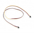
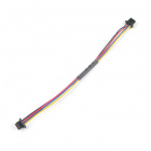
You will also need at least one Qwiic cable to connect your Qwiic Dual Solid State Relay to your microcontroller:


Required Tools
With the Qwiic system, soldering is not required to use the Qwiic Dual Solid State Relay but you will need a pair of wire strippers and a screwdriver to assemble your AC load.


Suggested Reading
If you aren't familiar with the Qwiic system, we recommend reading here for an overview:
We would also recommend reading through the following tutorials if you are not familiar with the concepts covered in them:
Serial Communication
Electric Power
Hardware Overview
The SparkFun Qwiic Dual Solid State Relay is built on a similar design to our Qwiic Quad Relay and uses an ATTiny84 to act as the "brain" for the board. To allow for faster and quieter switching of the load, this board uses solid state relays instead of electromechanical relays. The ATTiny84 comes pre-programmed with firmware to accept commands via I2C from an attached microcontroller so you can keep other I/O pins free for other uses.
In this section we'll cover the hardware present on the Qwiic Dual Solid State Relay and note some of the unique functionality of the components.
Solid State vs Mechanical Relays
Let's talk briefly about two types of relays before we get into the details on the solid state relays included with the kit. A relay is a special kind of switch that has a switching mechanism inside isolated from the switch. This allows us to control the high-output side of the relay from a low-power input like a microcontroller.
Now, when it comes to the comparing an electromechanical relay (EMR) and a solid state relay (SSR), the primary difference is an EMR uses an electromagnetic field to physically close a mechanical switch inside the relay where an SSR uses a semiconductor like a MOSFET or an opto-isolator to switch the load on and off. This allows the SSR to switch at much higher speeds than an EMR and also increases their durability since there are no moving parts inside. Theoretically, and if used within spec, an SSR can last forever where EMR's are designed with an expected lifetime. EMR's are typically cheaper and also can allow multiple loads on a single relay (if it has multiple contacts) where SSR's are limited to a single load.
There is a lot of discussion out there about which type of relay is best but it really comes down to two things: budget and versatility. This brief outline covers the very basics of electromechanical and solid state relays so with some more research you can decide which type of relay will be best suited for your project. For a short yet informative overview of electromechanical relays, check out this section of our Qwiic Quad Relay Hookup Guide.
SSRF-240D25 Solid State Relays
The board includes two PCB-mount SSRF-240D25 solid state relays from Tyco Electronics. Let's cover some characteristics from the relay's datasheet so you know what to expect from them and the Dual Solid State Relay.
| Characteristic | Range |
|---|---|
| Input Voltage | 3V-15V |
| Supply Current | 15mA @5V (20 mA @3.3V) |
| Load Voltage | 12-280VAC |
| Max Current (Through Relay) | 25A (@240 VAC) |

The relays use the Zero Voltage Cross trigger method so when operating on a 60Hz AC carrier signal you can switch the relays up to 120 times per second! Read on in the Arduino Examples section where we'll demonstrate how to do that using a PWM signal.
Both relays' outputs are tied to their own 2-pin screw terminal so all you need to connect your load is a pair of wire strippers and a screwdriver. We've also included two footprints so you can solder 5mm LEDs to act as indicators for when the load is powered.
One last note before we move on from the relays. The relay control circuit is designed for a Normally Open circuit only. This means your load is normally off until the relay is switched on. For more information on how this circuit is configured, check out the schematic and the relay datasheet.
ATTiny84
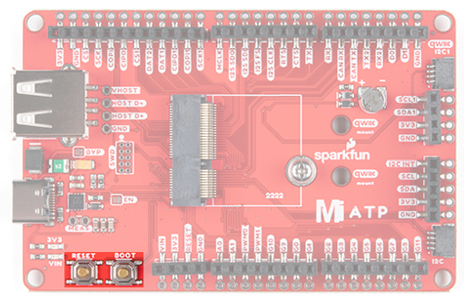
The ATTiny84 comes pre-programmed with firmware to control the two relays on the board via I2C commands. The ATTiny84's I2C address is 0x0A by default. There is also a 2x3 header broken out on the back of the board for programming the ATTiny84. This is primarily used for programming during manufacturing but you can re-program the IC if you would like. You an download and modify the firmware from the Hardware GitHub repo.

Power
Power for the board is provided either via the Qwiic interface or through the labeled 3.3V and GND pins broken out on the bottom left of the board.
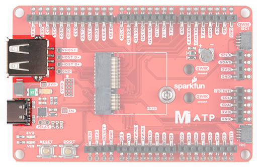
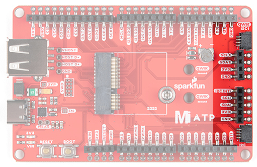
Qwiic and I2C Interface
The I2C interface is broken out to two Qwiic connectors on either side of the board as well as 0.1"-spaced header pins for those who prefer a more traditional soldered connection. We have also broken out the ATTiny84's reset pin in case you would like to reset the IC without resetting your entire circuit.

Jumpers
There are three jumpers on the Qwiic Dual Relay labeled PWR, I2C and ADR. The PWR jumper enables the Power LED, the I2C jumper pulls the SDA and SCL lines to 3.3V and the ADR jumper sets the I2C address of the ATTiny84.

Power Jumper
The power jumper (labeled PWR) controls voltage to the power LED on the board. This jumper is closed by default. To disable the power LED, simply open the jumper by severing the trace in between the two pads. Disabling the power LED can help reduce the total current draw of the board.
Address Jumper
The address jumper (labeled ADR) sets the I2C address for the ATTiny84. The jumper is closed by default with the address set to 0x0A. Opening the jumper will change the address to 0x0B.
I2C Jumper
The I2C Jumper pulls the SDA and SCL lines to 3.3V via two 4.7K Ohm resistors. The jumper is closed by default. Open this jumper if you have multiple sensors connected to the bus with their own pull-up resistors enabled to avoid causing the parallel equivalent resistance creating too strong of a pull-up for the bus to operate correctly. As a general rule, disable all but one pair of pull-up resistors if multiple devices are connected to the bus.
Board Dimensions
The Qwiic Dual Solid State Relay measures 3.55" x 2.65" (90.17mm x 67.31mm) and includes nine mounting holes that fit a 4-40 screw so you have plenty of mounting options.

With all the hardware included with the Qwiic Dual Solid State Relay covered, now it's time to connect it to your microcontroller and assemble your high voltage load circuit.
Hardware Assembly
With SparkFun's Qwiic ecosystem, connecting the Dual Solid State Relay to your circuit is a breeze! Before we connect the Dual SSR to your microcontroller circuit, we'll want to prepare and assembly our AC load(s) and connect them to the screw terminals for each relay.
Output Load Assembly
Next up we'll want to prepare our AC load we are controlling with the relays. This assembly requires you to cut and strip wire for your AC load. If you need help or tips for working with wire take a look at this tutorial:
You'll have to cut and strip one of the wires on your load AC line and then connect the cut ends to the relay you intend to use with your load. Make sure the cable is NOT plugged into the wall as you cut into the wire. After your wire is cut and stripped, connect the ends to the screw terminal for one of the relays and use a screwdriver to tighten them securely. Repeat the process for your second AC load.
If you need tips or help on safety and insulation on high voltage circuits, check out the notes about Safety and Insulation from our Beefcake Relay Control Kit.
Connecting to Microcontroller
Once the AC side of your circuit is assembled, we can go ahead and plug everything in. Plug one end of a Qwiic cable into your Relay board and the other into the Qwiic connector on your microcontroller. If your chosen microcontroller is not Qwiic-enabled, you can use something like this Qwiic adapter cable to make the proper connections to your microcontroller's I2C pins.

Alternatively, you can use the PTH pins broken out on the board but you will need to solder to them for a proper connection. If you are not familiar with through-hole soldering take a look at this tutorial:
How to Solder: Through-Hole Soldering
September 19, 2013
Now that our Qwiic Dual Solid State Relay connected to the microcontroller and the A/C load(s) is prepared and connected securely to a relay, it's time to upload some code to switch it on and off.
Qwiic Relay Arduino Library
The SparkFun Qwiic Relay Arduino Library works with all SparkFun Qwiic Relay boards to help you use your Qwiic Relay to its full functionality. You can click the link below to download the file or navigate through the Arduino Library Manager by searching SparkFun Qwiic Relay. You can also go the Github page and get it directly.
Library Functions
The list below outlines all of the functions of the Qwiic Relay library along with short descriptions of what they do. The examples cover nearly all of the functions so we recommend referring to them for help integrating the functions into your own code.
These functions will work with all SparkFun Qwiic Relay boards.
bool begin(TwoWire &wirePort = Wire);- Initialize the Qwiic Relay on the I2C busfloat singleRelayVersion();- Returns the version number of the firmware present on your relay board.void turnRelayOn(uint8_t relay);- Turn the given relay on. For example,turnRelayOn(1);will toggle the first relay.void turnRelayOff(uint8_t relay);- Turn the selected relay off. Similar to the above function, select values between 1 and 4 to turn the chosen relay off.void toggleRelay(uint8_relay)- Toggles the selected relay to the opposite state. The function first checks the status of the relay and is toggled to eitheronoroffdepending on what the status check returns.void turnAllRelaysOn();- Turns all relays on the board on.void turnAllRelaysOff();- Turns all relays on the board off.void toggleAllRelays();- Toggles all relays on the board to the opposite state.uint8_t getState(uint8_t relay);- Returns the status of the selected relay. Returns1if on or0if off.bool changeAddress(uint8_t newAddress);- Changes the I2C address of the Qwiic Relay. The new address is written to the memory location in EEPROM that determines the address.
The below function is intended for the Qwiic Solid State Relay boards only. It will not work on either of the Qwiic Mechanical Relay boards.
bool setSlowPWM(uint8_t relay, uint8_t pwmValue);- Starts a slow PWM (1Hz) with a range from 0-120 for the selected relay. The PWM range is limited to 0-120 as this is the maximum PWM resolution for Zero-crossing SSR's at 60Hz. SettingpwmValueto 120 will give you 100% duty cycle and continuously keep the selected relay switched on.
Arduino Examples
The examples included with the SparkFun Qwiic Relay Arduino Library work with all Qwiic Relay boards with one exception. Example 7 - Slow PWM was added specifically for the two Qwiic Solid State Relay boards to demonstrate how to use the setSlowPWM(uint8_t relay, uint8_t pwmValue); function. As mentioned in the previous section, this function will only work on the SSR boards and not the EMR boards. In this section we'll explore this example to explain how it works and how to modify it.
Also, take note that depending on which Qwiic Relay board you are using, you'll need to alter the I2C address definition in the beginning of all of the examples. Below you can see the proper definition for the default address on the Qwiic Dual Solid State Relay:
language:c
#define RELAY_ADDR 0x0A
If you have altered the ADR jumper or changed the I2C address using the bool changeAddress(uint8_t newAddress); function, adjust the above definition accordingly.
One last note before we move into the example. This example was originally written for the Quad Solid State Relay Kit and defines the relay object, Qwiic_Relay, as quadRelay(RELAY_ADDR); which may be a bit confusing if you are not using that kit. The code will work just fine with that object definition but if you would prefer, you can alter that object to something else. If you do alter this definition, you will need to replace that object call in each function that uses the old one. The code below demonstrates these modifications to Example 7.
Example 7 - Slow PWM
This example generates a Pulse Width Modulation (PWM) signal from the ATTiny84 on the board to quickly switch a selected relay on and off. Note, the code below is NOT identical to Example7_Slow_PWM. This example was originally written for the Qwiic Quad Solid State Relay Kit and sets slowPWM values for four relays so we've included a modified version below that sets up only two relays and also uses the default I2C address for the Dual Solid State Relay.
You can copy the code below and paste it into a new Arduino sketch or, if you you prefer, you can open the default example in Arduino by navigating to File>Examples>SparkFun Qwiic Relay Arduino Library>Example7_Slow_PWM. Next, open the Tools menu and select your board (in our case, Arduino Uno) and the correct Port your board enumerated on.
language:c
#include <Wire.h>
#include "SparkFun_Qwiic_Relay.h"

#define RELAY_ADDR 0x0A // Alternate address 0x0B


Qwiic_Relay dualRelay(RELAY_ADDR);

void setup()
{
  Wire.begin();
  Serial.begin(115200);

  // Let's make sure the hardware is set up correctly.
  if(!dualRelay.begin())
    Serial.println("Check connections to Qwiic Relay.");
  else
    Serial.println("Ready to flip some switches.");

  Serial.println("Let's turn each relay on, one at a time.");
  // To turn on a relay give the function the number you want to turn on (or
  // off).

 dualRelay.setSlowPWM(1, 75);
 dualRelay.setSlowPWM(2, 75);
 Serial.println(dualRelay.getSlowPWM(1));
 Serial.println(dualRelay.getSlowPWM(2));


}

void loop()
{
}
Upload the code and open your serial monitor with the baud set to 115200. The code prints out whether or not the initialization of the Qwiic Dual SSR was successful and then prints the PWM value for each relay set using the setSlowPWM(); function. Let's take a closer look at the code.
The code sets up each relay to run at a default PWM value of 75 (62.5% duty-cycle). Try playing around with the PWM values set in the setSlowPWM(); function for each relay to see how it affects the behavior of your load(s).
language:c
// To turn on a relay give the function the number you want to turn on (or
// off).
quadRelay.setSlowPWM(1, 75);
quadRelay.setSlowPWM(2, 75);
Note, as we mentioned in the previous section, the PWM resolution is capped at 120 since the relay cannot switch more times than that in one second on a 60Hz signal.
The code also demonstrates how to use the getSlowPWM(); function by printing out the PWM value set for each relay:
language:c
Serial.println(quadRelay.getSlowPWM(1));
Serial.println(quadRelay.getSlowPWM(2));
If Arduino isn't your jam, head on to the next section where we cover the Python package for this and our other Qwiic Relay boards.
Qwiic Relay Python Package
Note: This example assumes you are using the latest version of Python 3. If this is your first time using Python or I2C hardware on a Raspberry Pi, please checkout our tutorial on Python Programming with the Raspberry Pi and the Raspberry Pi SPI and I2C Tutorial.
We've written a Python package to control the Qwiic Relay family including the Qwiic Dual Solid State Relay. You can install the sparkfun-qwiic-relay Python package hosted by PyPi through a command interface. If you prefer to manually download and build the libraries from the GitHub repository, you can download the package by clicking the button below:
(*Please be aware of any package dependencies. You can also check out the repository documentation page, hosted on Read the Docs.)
Installation
Note: Don't forget to double check that the hardware I2C connection is enabled on your Raspberry Pi or other single board computer. The Raspberry Pi tutorials linked in the note above cover how to enable the Pi's I2C bus.
PyPi Installation
This repository is hosted on PyPi as the sparkfun-qwiic-relay package. On systems that support PyPi installation via pip3 (use pip for Python 2) is simple using the following commands:
For all users (Note: the user must have sudo privileges):
language:bash
sudo pip3 install sparkfun-qwiic-relay
For the current user:
language:bash
pip3 install sparkfun-qwiic-relay
Local Installation
To install, make sure the setuptools package is installed on the system.
Direct installation at the command line (use python for Python 2):
language:bash
python3 setup.py install
To build a package for use with pip3:
language:bash
python3 setup.py sdist
A package file is built and placed in a subdirectory called dist. This package file can be installed using pip3.
language:bash
cd dist
pip3 install sparkfun_qwiic_relay-<version>.tar.gz
Dependencies
This Python package has a few dependencies in the code, listed below:
language:python
from __future__ import print_function
import math
import qwiic_i2c
Function Overview
For a full overview of all the functions included with the Qwiic Relay Py package, head on over to the ReadtheDocs page.
Python Examples
Now that you have the Qwiic Relay Py package installed, it's time to check out the examples included with the package.
Qwiic_Relay_ex1 - The Basics
This example demonstrates the basics of turning relays on and off and reading relays' statuses. The code initializes the Dual SSR on the I2C bus and steps through the different ways to turn both relays on and off and shows how to read the status of both relays.
The example was written to work by default with the Qwiic Quad Relay Kit so we'll need to modify the I2C address call and we'll also want to remove references to a third and fourth relay. The code below is NOT the same as qwiic_relay_ex1.py and has been modified to work with the Dual SSR board. Copy the code below or you can open the example from your install of the Qwiic Relay Python package:
language:python
from __future__ import print_function
import qwiic_relay
import time
import sys


QUAD_RELAY = 0x6D
SINGLE_RELAY = 0x18
QUAD_SOLID_STATE_RELAY = 0x08
DUAL_SOLID_STATE_RELAY = 0x0A

#Be sure to initialize your relay with the proper address.
myRelays = qwiic_relay.QwiicRelay(DUAL_SOLID_STATE_RELAY)

def runExample():

    print("\nSparkFun Qwiic Relay Example 1\n")

    if myRelays.begin() == False:
        print("The Qwiic Relay isn't connected to the system. Please check your connection", \
            file=sys.stderr)
        return

    #Turn on relays one and two
    myRelays.set_relay_on(1)
    myRelays.set_relay_on(2)
    time.sleep(1)

    #Print the status of all relays
    for relayNum in range(2):
        current_status = None
        if myRelays.get_relay_state(relayNum) is True:
            current_status = "On"
        else:
            current_status = "Off"
        print("Status 1: " + current_status + "\n")

    #Turn off 1 and turn on 2
    myRelays.set_relay_off(1)
    myRelays.set_relay_on(2)
    time.sleep(1)


    #Turn all relays on, then turn them all off
    myRelays.set_all_relays_on()
    time.sleep(1)

    myRelays.set_all_relays_off()


if __name__ == '__main__':
    try:
        runExample()
    except (KeyboardInterrupt, SystemExit) as exErr:
        print("\nEnding Example 1")
        sys.exit(0)
Example 2 - Slow PWM
The second example included with the Python package demonstrates how to use the set_slow_pwm() function. The example starts just like the first by initializing the Dual SSR on the I2C bus and then sets the PWM duty-cycle for each relay and uses the get_slow_pwm() function to print the PWM value set for each relay.
Just like Example 1, this was written to work by default with the Qwiic Quad Relay Kit so modify the I2C address call and remove references to a third and fourth relay like above. Similarly, the code below is NOT the same as qwiic_relay_ex2.py and has been modified to work with the Dual SSR board. Copy the code below or you can open the example from your install of the Qwiic Relay Python package and modify it to work with your Dual SSR:
language:python
from __future__ import print_function
import qwiic_relay
import time
import sys

QUAD_RELAY = 0x6D
SINGLE_RELAY = 0x18
QUAD_SOLID_STATE_RELAY = 0x08
DUAL_SOLID_STATE_RELAY = 0x0A

#Be sure to initialize your relay with the proper address.
myRelays = qwiic_relay.QwiicRelay(DUAL_SOLID_STATE_RELAY)

def runExample():

    print("\nSparkFun Qwiic Relay Example 2\n")

    if myRelays.begin() == False:
        print("The Qwiic Relay isn't connected to the system. Please check your connection", \
            file=sys.stderr)
        return

    #Note that our range is 0-120 for setting a PWM value as there are only 120 times where the zero crossing relay can switch in one second

    myRelays.set_slow_pwm(1, 30) #25% duty cycle
    myRelays.set_slow_pwm(2, 60) #50% duty cycle

    #Print out our PWM values
    for relayNum in range(1, 5):
        pwmValue = myRelays.get_slow_pwm(relayNum)
        print("PWM Value for relay " + str(relayNum) + ": " + str(pwmValue))
    #Let the slow PWM run for a while
    time.sleep(15)


    #Set all relays off
    myRelays.set_slow_pwm(1, 0)
    myRelays.set_slow_pwm(2, 0)

if __name__ == '__main__':
    try:
        runExample()
    except (KeyboardInterrupt, SystemExit) as exErr:
        print("\nEnding Example 1")
        sys.exit(0)
Each relay is set to a different duty cycle to demonstrate how that affects the behavior of the load and will run for 15 seconds. Want your relay to pulse at a 50% duty cycle? Set the slow PWM value to 60. Note: Just like the Arduino Library, the PWM resolution is limited to 0-120 since there are only 120 times where the zero crossing relay can switch in one second.
That's all for the basics of our Python package! Try using the various functions included here to write your own code for your next relay project.
Resources and Going Further
For more information, take a look through the resources below:
- Schematic (PDF)
- Eagle Files (ZIP)
- Board Dimensions (PNG)
- Relay Datasheet (PDF)
- Hardware GitHub Repo
- Qwiic Relay Arduino Library
- Qwiic Relay Python Package
Looking for inspiration for your next power control project? Check out these other Power tutorials from SparkFun:
Single Supply Logic Level Converter Hookup Guide
LuMini 8x8 Matrix Hookup Guide
Beginner Parts Kit Identification Guide
LiPo Charger Plus Hookup Guide
learn.sparkfun.com | CC BY-SA 3.0 | SparkFun Electronics | Niwot, Colorado